Molecular wire crossbar memory

Inactive Publication Date: 2000-10-03
RGT UNIV OF CALIFORNIA +1
View PDF9 Cites 1075 Cited by
  • Summary
  • Abstract
  • Description
  • Claims
  • Application Information

AI Technical Summary

Benefits of technology

In accordance with the present invention, a molecular wire crossbar memory (MWCM) system is provided. The MWCM comprises a two-dimensional array of a plurality of nanometer-scale devices, each device comprising a junction formed by a pair of crossed wires where one wire crosses another and at least one connector species connecting the pair of crossed wires in the junction. The connector species comprises a bi-stable molecular switch. The junction forms either a resistor or a diode or an asymmetric non-linear resistor. The junction has a state that is capable of being altered or sensed by application of a voltage. The reading (sensing) voltage is of a non-destructive value, so as to avoid switching the state of the junction.
The physical advantages of the MWCM are in its scalability, low power consumption, the fact the switching elements have well-defined threshold voltages, low sensitivity to fields and temperature, and the read process is non-destructive. It is expected that as this architecture matures, it will eventually utilize carbon nanotubes, which have a diameter of about 1 nm and will certainly define the wiring limit for electronic devices. The MWCM is basically a voltage-controlled device, and therefore the fact that it contains components with relatively large resistance is actually an advantage in terms of power consumption. Also, the redox reactions that will be utilized as the switching elements at the crosspoints are voltage initiated, with values typically between 0.5 and 1 V. In fact, these threshold voltages are so reproducible that the technique of cyclic voltammetry, i.e. measuring the "waves" or steps in the I-V curve for such a redox reaction, has been used by chemists for decades as an analytical technique to determine what types of functional groups are present on an "unknown" molecule. Also, the size of the voltage required to change the state of the bit means the bit should be stable up to temperatures that would destroy the entire device, so the memory bits themselves will not be the most sensitive component of a system. Finally, the read of the bit is accomplished by determining the junction resistance by monitoring the tunneling current. The voltage used for the read process will be lower than that required to change the oxidation state of the switch molecules, so there will not be any problem with destroying the sense of the bit on reading it.
MWCM has significant advantages over both MRAM and FeRAM. MWCM scales to much higher bit densities than the ultimate expected for either MRAM or FeRAM. Perhaps even more significant is the fact that a MWCM needs much less power than MRAM, which requires relatively large currents to set the sense of a bit.

Problems solved by technology

However, because of a combination of physical and economic reasons, the miniaturization that has accompanied the growth of Si ICs is reaching its limit.
The major problem with (1) is that the wafer on which the devices are built must be aligned to within a fraction of a nanometer in at least two dimensions for several successive stages of lithography, followed by etching or deposition to build the devices.
This level of control will be extremely expensive to implement.
The major problem with (2) is that it is a serial process, and direct writing a wafer full of complex devices, each containing trillions of components, could well require many years.
Finally, the problem with (3) is that the only known chemical analogues of high information content circuits are proteins and DNA, which both have extremely complex and, to date, unpredictable secondary and tertiary structures that causes them to twist into helices, fold into sheets, and form other complex 3D structures that will have a significant and usually deleterious effect on their desired electrical properties as well as make interfacing them to the outside world impossible.
The primary disadvantages of MRAM are that the spin-tunneling switch that is used to store individual bits at present only has about a 30% difference in resistance between the ON and OFF state, which means that memories must either be small or relatively slow to be read reliably.
Such memories also would be damaged either by strong magnetic fields or by high temperatures, either of which can erase the memory.
Finally, relatively large currents are required to set the sense of a bit, and this leads to problems with designing the electrical circuitry that accompanies the MRAM and also with the power consumption of the device.
There were also significant early attempts to build cross-point memories using ferroelectrics, but these were unsuccessful.
The primary problem with ferroelectric cross-point memories has been crosstalk between memory elements--a phenomenon referred to as the `half-select disturb-pulse`.
This occurred because of the fundamental properties of ferroelectrics, which do not have a sharp switching threshold voltage (they switch when a coercive field is exceeded, and there are many issues that vary the voltage required to achieve that field).
Another annoying issue with FeRAM is that reading a cell will necessarily destroy a bit if it is set "ON", and thus reading actually requires a read-rewrite cycle, which adds to the complexity, temporal overhead, and power consumption of the devices.

Method used


Image

  • Molecular wire crossbar memory
  • Molecular wire crossbar memory
  • Molecular wire crossbar memory

Examples


example

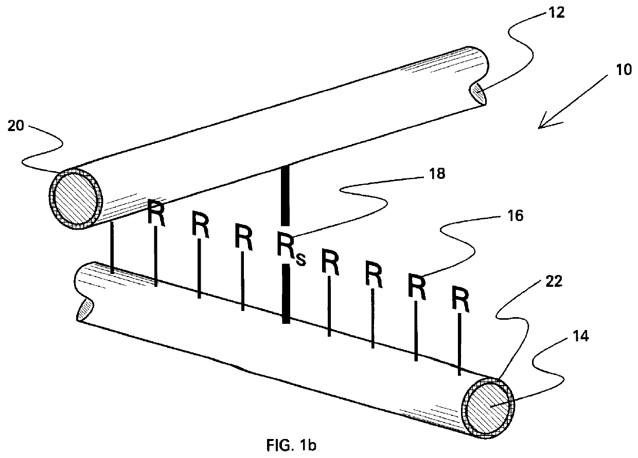
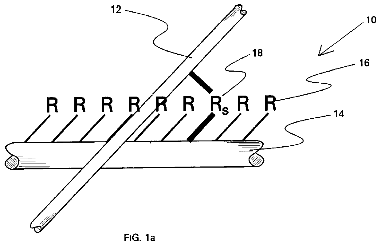
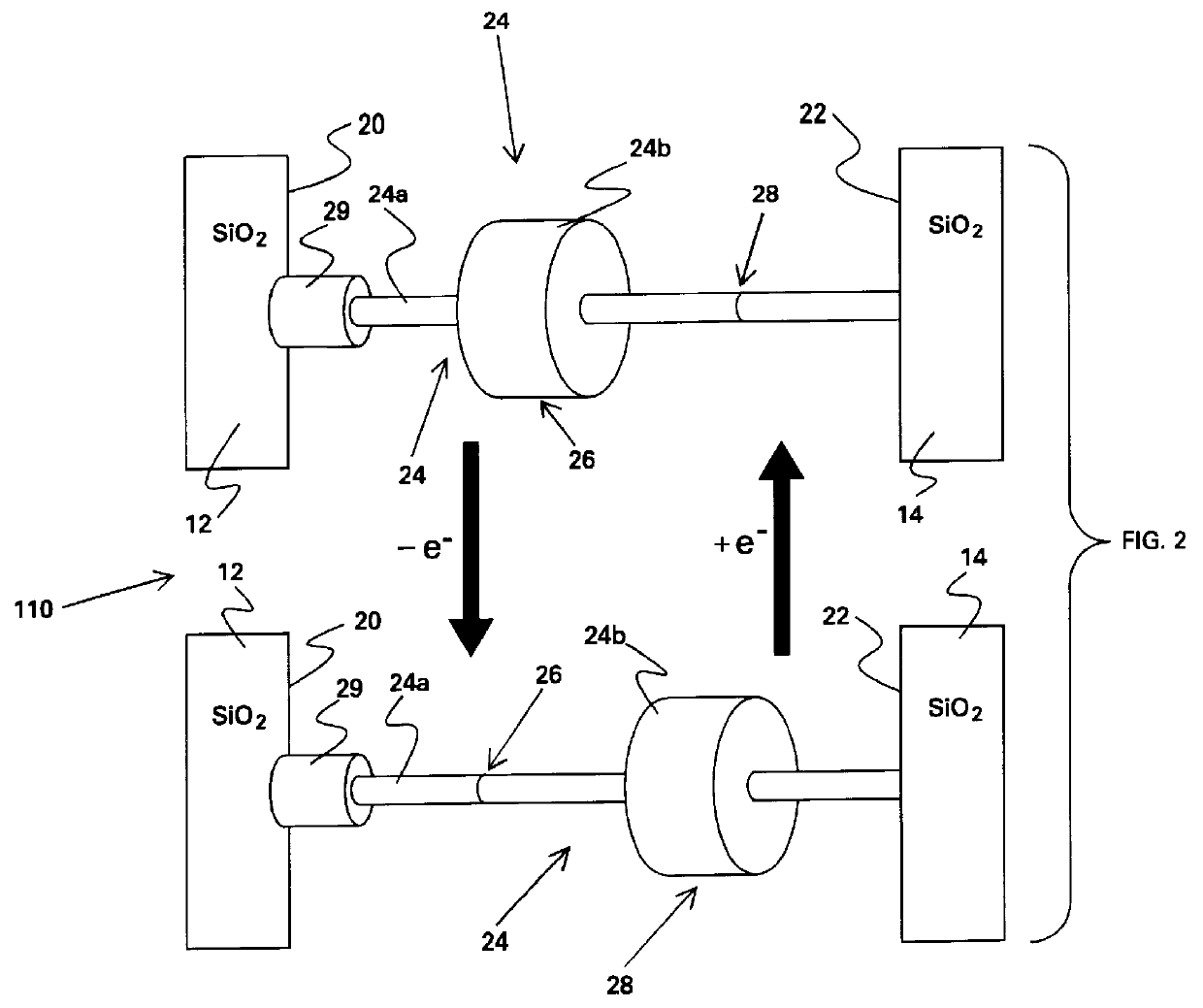
A molecular switch-based device that could be configured as an electrically configurable read-only-memory bit was fabricated. The device was made as follows: a 5 micrometer wide aluminum wire 12 was deposited on a silica substrate using conventional lithographic procedures. The wire 12 was provided with an oxide coating 14 of Al.sub.2 O.sub.3, which naturally formed to a thickness of about 1.0 to 1.5 nm when the aluminum wire was exposed to air. One of the molecular species shown in FIGS. 8A-8C was dissolved in tetrahydrofuran solvent, prepared as a Langmuir monolayer, and transferred as a Langmuir-Blodgett single molecular monolayer film 16 that covered the Al wire 12 and a silica substrate. The molecular compounds 24 shown in FIGS. 8A-8C are from a class of molecular compounds known as rotaxanes. Each molecular compound consists of a dumbbell component, or backbone, 24a, a counterion 36, and 0, 1, or 2 (bis-para-phenylene-34-crown-10) rings 24b (FIGS. 8A, 8C, and 8B, respectively)...


PUM


Abstract

A molecular wire crossbar memory (MWCM) system is provided. The MWCM comprises a two-dimensional array of a plurality of nanometer-scale devices, each device comprising a junction formed by a pair of crossed wires where one wire crosses another and at least one connector species connecting the pair of crossed wires in the junction. The connector species comprises a bi-stable molecular switch. The junction forms either a resistor or a diode or an asymmetric non-linear resistor. The junction has a state that is capable of being altered by application of a first voltage and sensed by application of a second, non-destructive voltage.

Description

The present application is related to the following applications: Ser. Nos. 09 / 282,045 ("Molecular Wire Crossbar Logic") [PD-10981969-1] 09 / 280,225 ("Molecular Wire Crossbar Interconnect") [PD-10981966-1] 09 / 282,049 ("Demultiplexer for a Molecular Wire Crossbar Network") [PD-10981970-1]; and 09 / 292,767 ("Chemically Synthesized and Assembled Electronic Devices") [PD-10981071-1], all filed on even date herewith. The present application employs the chemical synthesis and assembly techniques disclosed and claimed in 09 / 282,048 [PD-10981971-1] and the crossbar interconnections disclosed and claimed in 09 / 280,225 [PD-10981966-1].The present invention relates generally to electronic devices whose functional length scales are measured in nanometers, and, more particularly, to memory devices based on crossed wires joined by bi-stable molecules at the intersecting junctions.The silicon (Si) integrated circuit (IC) has dominated electronics and has helped it grow to become one of the world's l...

Claims


Application Information

Patent Timeline
IPC IPC(8): G11C13/02G11C11/36H01L27/28G11C11/14H01L51/00
CPCB82Y10/00G11C11/14G11C13/0009G11C13/025Y10S977/943G11C2213/81H01L27/28H01L51/0595G11C2213/77H10K19/00H10K10/701
Inventor KUEKES, PHILIP J.WILLIAMS, R. STANLEYHEATH, JAMES R.
Owner RGT UNIV OF CALIFORNIA
Why Eureka
Try Eureka