
Method for providing electrically fusible links in copper interconnection

a copper interconnection and electrical fusible technology, applied in the field of fuselinks, can solve the problems of not being able to meet the requirements of copper metallurgy, high current is not compatible with low-voltage ic technology, and gold is not compatible with aluminum interconnection metallurgy widely used,

Inactive Publication Date: 2000-03-07
GOOGLE LLC
View PDF8 Cites 159 Cited by
  • Summary
  • Abstract
  • Description
  • Claims
  • Application Information

AI Technical Summary

Benefits of technology

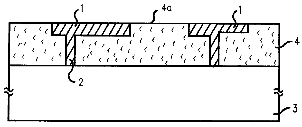
FIG. 1 is a simplified cross-sectional view of a conventional semiconductor s...

Problems solved by technology

Further, platinum or gold is not compatible with the widely used aluminum interconnection metallurgy.
In the Soden and Greig fuse, hundreds of miliamps of current is shown to be required to blow the fuse; such high current is not compatible with low voltage IC technologies.
This method is not applicable to copper metallurgy which requires a Damascene method.
This method is not compatible with the current metallurgical schemes, all of which require an underlayer.
Further, the interface formed between the top and the bottom half of the interconnection thickness is known to be preferred sites for void accumulation causing degraded reliability.
Fischer's scheme is also incompatible with processes required for copper metallurgy.
This results in an inconsistent amount of tungsten being left along the sidewalls of the fuse recess resulting in poor fuse yield.
Such schemes necessarily make the desired electrical fuse blow techniques inoperable for many applications and one has to resort to a laser blow techniques.
The reason for such fuse material constrains is erroneously said to be process simplicity or cost effectiveness.
The laser blow operation, however, requires another mask application to remove the insulation layer above the fuse, requires expensive laser tools, adds logistics to keep track of which fuse in which chip is to be blown, and consumes more time than electrical fuse blow methods which could be automated with a device final test.
Despite repeated efforts in the prior art, however, problems of poor fabrication process yield, process incompatibility, ability for clean electrical fuse blow, etc., remain and better methods for making reliable fuse links need to be developed.

Method used


Image

  • Method for providing electrically fusible links in copper interconnection
  • Method for providing electrically fusible links in copper interconnection
  • Method for providing electrically fusible links in copper interconnection

Examples


Embodiment Construction

)

In describing the preferred embodiment of the present invention, reference will be made herein to FIGS. 1-4 of the drawings in which like numerals refer to like features of the invention. Features of the invention are not necessarily shown to scale in the drawings.

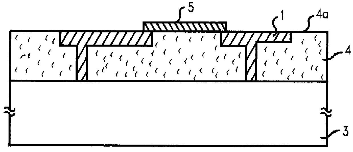
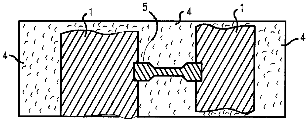
Referring now to FIG. 1 there is shown copper interconnection lines 1 and via studs 2 defined on a semiconductor substrate 3. It is understood that the substrate 3 is a semiconductor multilayer substrate having a plurality of semiconductor devices and lower levels of interconnection lines and contact studs defined by methods of the prior art. It is further understood that integrated lines 1 and via studs 2 are defined by a Double Damascene method of the prior art. In such damascene methods, interconnection lines 1 are essentially coplanar with the upper surface 4a of a surrounding insulating and passivating layer 4. The interconnection metallurgies typically contain a liner under the high conductivity metal or alloy (not ...


PUM


Abstract

A method is provided for the fabrication of fuses within a semiconductor IC structure, which fuses are delectable by a laser pulse or a low voltage electrical pulse typically below 3.5 V to reroute the electrical circuitry of the structure to remove a faulty element. The fuses are formed on the surface of circuitry which is coplanar with a surrounding dielectric such as the circuitry formed by a Damascene method. A preferred fuse material is silicon-chrome-oxygen and the preferred circuitry is copper.

Description

1. Field of the InventionThe present invention generally relates to the fabrication of microfuses within a semiconductor structure and, more specifically, to a fuselink and process of fabricating a fuselink which is compatible with advanced CMOS technology having copper interconnections defined by a Damascene method and 2.5 volt circuitry, which fuselinks would be delectable either by a laser pulse or by a low voltage electrical pulse.2. Description of Related ArtIn the fabrication of integrated circuit (IC) structures, fusible links play an important role in improving the yield of the fabrication process. In general, it is desirable to provide redundancy in certain elements of the circuitry of an electronic component and the faulty element could be removed via a fuse and the component still be used. Two types of such fuses are in use. In one type, the fuse element is blown using an external heat source, e.g., laser beam. In a second type, the fuse is blown by flowing an electrical ...

Claims


Application Information

Patent Timeline
IPC IPC(8): H01L23/52H01L23/525
CPCH01L23/5258H01L2224/13H01L24/05H01L2224/05001H01L2224/05008H01L2224/05024H01L2224/05568H01L2924/00014
Inventor AGARWALA, BIRENDRA N.DALAL, HORMAZDYAR M.NGUYEN, DU B.RATHORE, HAZARA S.
Owner GOOGLE LLC
Learn More