Silicon-controlled rectifier

a rectifier and silicon technology, applied in the direction of semiconductor devices, electrical equipment, transistors, etc., can solve the problems of occupying a considerable chip area, affecting the reliability of integrated circuits, and severely restricting the reliability of semiconductor products

Active Publication Date: 2022-09-15
POWERCHIP SEMICON MFG CORP
View PDF4 Cites 0 Cited by
  • Summary
  • Abstract
  • Description
  • Claims
  • Application Information

AI Technical Summary

Problems solved by technology

With the continuous improvement of integrated circuit technology, static discharges (ESD) have become a serious problem affecting the reliability of integrated circuits.
More than one-third of the reliability problems of integrated circuits are caused by ESD, which severely restrict the reliability of semiconductor products.
In terms of chip ESD protection design, the traditional ESD protection design takes up a considerable chip area and brings great cost pressure.
When the sustain voltage is lower than the operating voltage VDD of the chip, a serious problem is brought about: latch-up.
Due to current discharge of the surface parasitic transistor formed in the cross-over N+ region 102c (discharge path P1), the sustain voltage of the MLSCR is higher than the sustain voltage of traditional SCRs, but in most cases it is still not enough to achieve latch-up immunity.

Method used


Image

  • Silicon-controlled rectifier
  • Silicon-controlled rectifier
  • Silicon-controlled rectifier

Examples


first embodiment

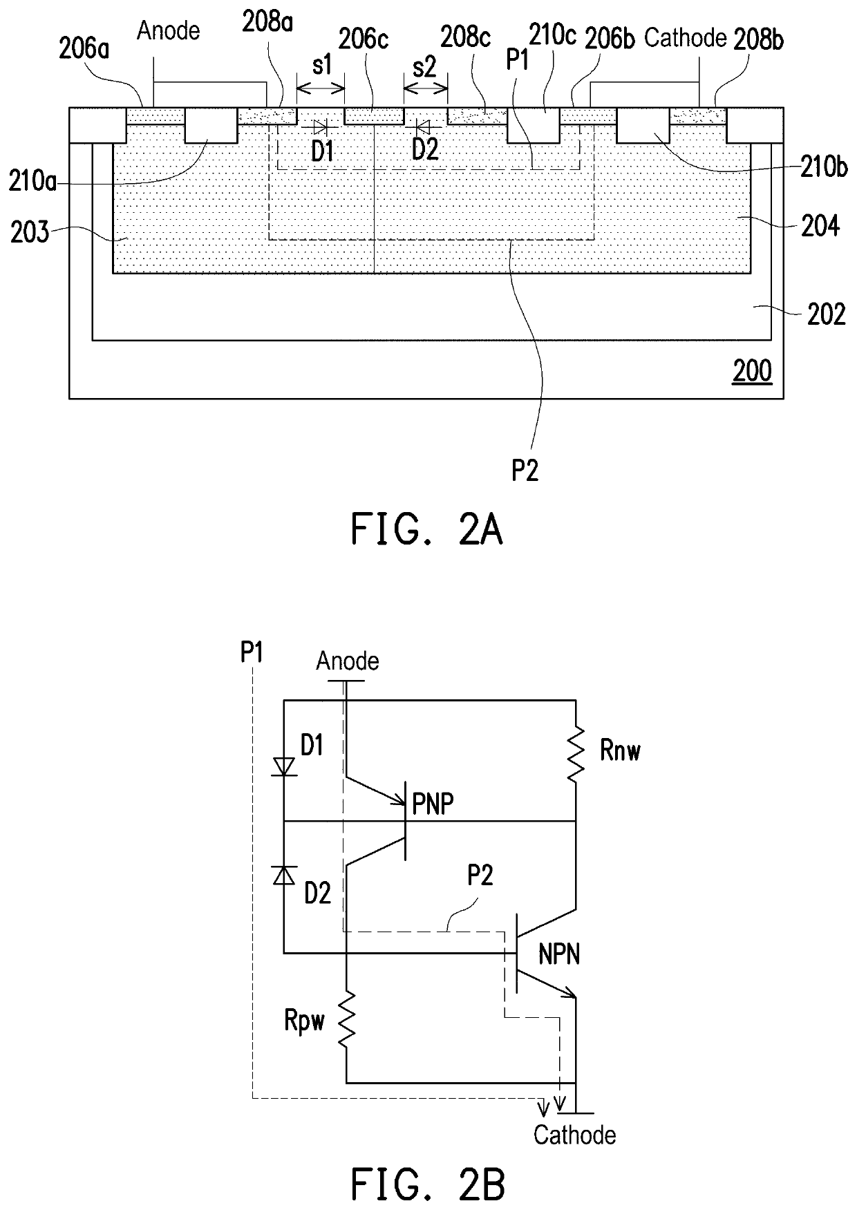
[0030]FIG. 2A is a cross-sectional diagram of a silicon-controller rectifier (SCR) according to the disclosure.

[0031]With reference to FIG. 2A, the SCR of the first embodiment is an enhanced diode-triggered silicon-controlled rectifier (EDTSCR), including: a substrate 200 of a first conductivity type; a deep well region 202 of a second conductivity type; a well region 204 of the first conductivity type; a well region 203 of the second conductivity type; a first heavily doped active region 208a of the first conductivity type; a second heavily doped active region 208b of the first conductivity type; a third heavily doped active region 208c of the first conductivity type; a first heavily doped active region 206a of the second conductivity type; a second heavily doped active region 206b of the second conductivity type; a third heavily doped active region 206c of the second conductivity type; a first shallow trench isolation structure 210a; a second shallow trench isolation structure 210...
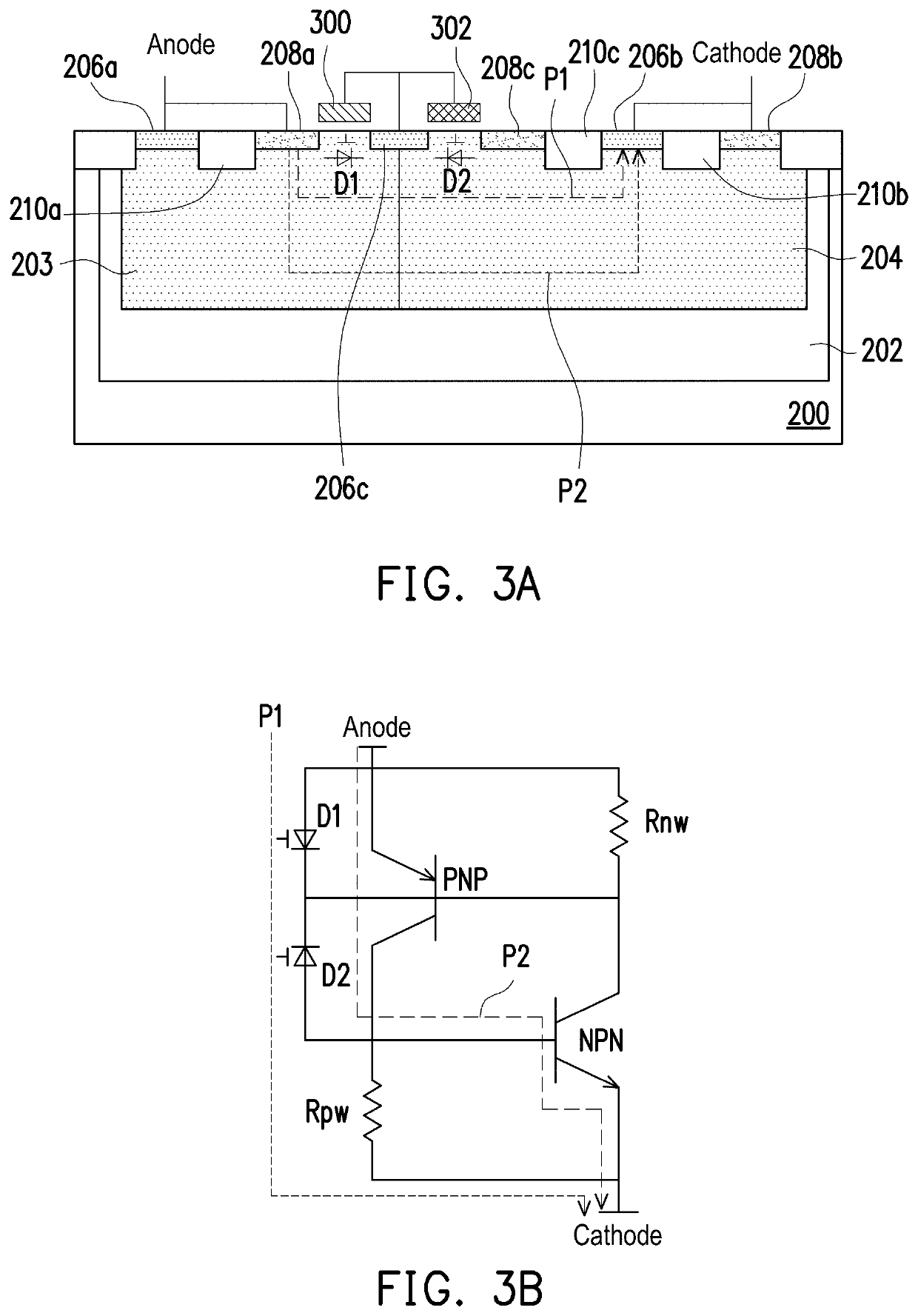
second embodiment

[0039]For the reverse diode D2, RC gate coupling effect by a gate capacitor and an N-well resistor helps to trigger the device. The gate capacitor is composed of the second gate 302, and the resistor is composed of the cross-over N+ region resistor and the N-well (the well region 203 of the second conductivity type) resistor. A gate voltage generated further enhances such effect, thereby improving the current discharge capacity of the forward (gate-controlled) diode D1 and the reverse (gate-controlled) diode D2. As a result, the SCR of the second embodiment can achieve a lower trigger and a faster response time under ESD pressure without using other trigger devices. Once the reverse diode D2 is turned on, the surface gate-controlled diode circuit (discharge path P1) starts to discharge the ESD current, and the parasitic transistor NPN will also be turned on. After the parasitic transistor NPN and the parasitic transistor PNP are turned on successively, finally the SCR path (the disc...


PUM

PropertyMeasurementUnit
widthaaaaaaaaaa
widthaaaaaaaaaa
voltageaaaaaaaaaa

Abstract

A silicon-controlled rectifier includes a substrate of a first conductivity type; a deep well region of a second conductivity type; a well regions of the first conductivity type and the second conductivity type; a first, second and third heavily doped active regions of the first conductivity type; a first, second and third heavily doped active regions of the second conductivity type; and a first, second and third shallow trench isolation structures. A reverse diode formed in the third heavily doped active region of the second conductivity type and the well region of the first conductivity type is embedded, and a forward diode is formed in the heavily doped active region of the first conductivity type and the well region of the second conductivity type. By sharing the third heavily doped active region of the second conductivity type across the well regions of different conductivity types, two back-to-back diodes are formed.

Description

CROSS-REFERENCE TO RELATED APPLICATION[0001]This application claims the priority benefit of China application serial no. 202110253917.2, filed on Mar. 9, 2021. The entirety of the above-mentioned patent application is hereby incorporated by reference herein and made a part of this specification.BACKGROUND1. Technical Field[0002]The disclosure relates to a semiconductor static protection technology, and particularly relates to a silicon-controlled rectifier (SCR) for unidirectional electro-static discharge (ESD) protection.2. Description of Related Art[0003]With the continuous improvement of integrated circuit technology, static discharges (ESD) have become a serious problem affecting the reliability of integrated circuits. More than one-third of the reliability problems of integrated circuits are caused by ESD, which severely restrict the reliability of semiconductor products. Therefore, it is essential to design effective ESD protection for integrated circuits.[0004]In terms of chi...

Claims


Application Information

Patent Timeline
Patent Type & Authority Applications(United States)
IPC IPC(8): H01L27/02
CPCH01L27/0262
Inventor LIOU, JUIN JEISONG, WENQIANGHO, CHING-SUNG
Owner POWERCHIP SEMICON MFG CORP
Why Eureka
Try Eureka