Double Control Gate Semi-Floating Gate Transistor and Method for Preparing the Same

Pending Publication Date: 2022-07-28
SHANGHAI HUALI INTEGRATED CIRCUIT CORP
View PDF3 Cites 0 Cited by
  • Summary
  • Abstract
  • Description
  • Claims
  • Application Information

AI Technical Summary

Benefits of technology

The double control gate semi-floating gate transistor and the method for preparing it described in this patent can improve the performance of the transistor by using high-K dielectric material and metal gate. This can reduce the quantum tunneling effect of the gate dielectric layer during charging of the floating gate and improve the gate leakage and power consumption. The polysilicon gate can also obtain better electric field control during reading and writing of the device. Additionally, the polysilicon control gate and metal control gate can work independently, allowing the device to achieve both reading and writing functions simultaneously.

Problems solved by technology

With the decrease of the size of semiconductor devices to process nodes of 28 nm and less than 28 nm, the thickness of gate dielectric layer SiON is reduced to less than 2 nm, which leads to the increase of the leakage current of the device.

Method used


Image

  • Double Control Gate Semi-Floating Gate Transistor and Method for Preparing the Same
  • Double Control Gate Semi-Floating Gate Transistor and Method for Preparing the Same
  • Double Control Gate Semi-Floating Gate Transistor and Method for Preparing the Same

Examples


Embodiment Construction

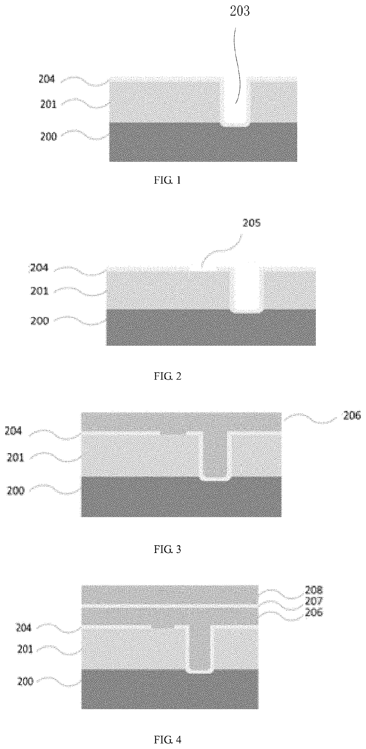
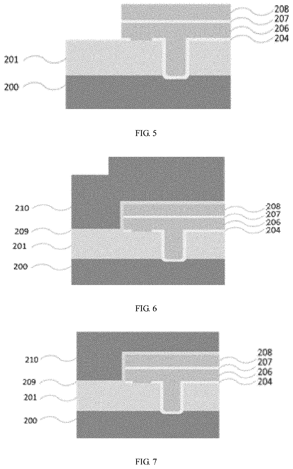
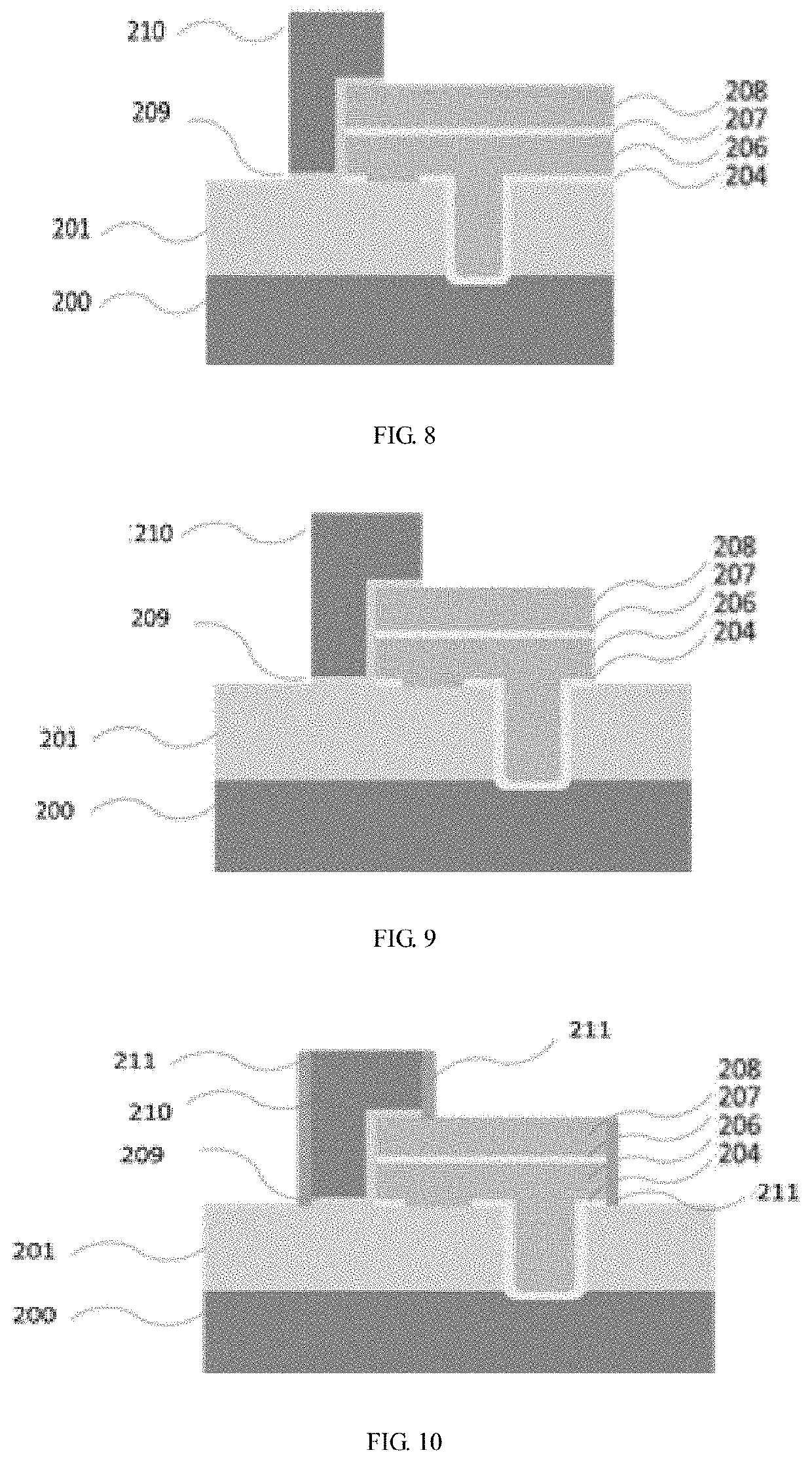
[0046]The embodiments of the present application will be described below through specific examples, and those skilled in the art can easily understand other advantages and effects of the present application from the content disclosed in the description. The present application may also be implemented or applied through other different specific embodiments, and the details in the description may also be modified or changed based on different views and applications without departing from the spirit of the present application.

[0047]Please refer to FIG. 1-FIG. 11. It should be noted that the drawings provided in the embodiment only are only used for schematically describing the basic concept of the present application, so the components related to the present application are only illustrated in the drawings, rather than are drawn according to the number, shape and size of the components in actual implementation. The pattern, number and scale of each component in actual implementation ma...


PUM


Abstract

The present application provides a double control gate semi-floating gate transistor and a method for preparing the same. A lightly doped well region provided with a U-shaped groove is located on a substrate; one part of a floating gate oxide layer covers sidewalls and a bottom of the U-shaped groove, the other part covers the lightly doped well region on one side, and the floating gate oxide layer covering the lightly doped well region; a floating gate polysilicon layer is filled in the U-shaped groove and covers the floating gate oxide layer; a polysilicon control gate stack includes a polysilicon control gate oxide layer on the floating gate polysilicon layer and a polysilicon control gate polysilicon layer on the polysilicon control gate oxide layer; a metal control gate stack includes a high-K dielectric layer and a metal gate.

Description

CROSS-REFERENCES TO RELATED APPLICATIONS[0001]This application claims priority to Chinese patent application No. 202110115619.7, filed on Jan. 28, 2021, and entitled “Double Control Gate Semi-Floating Gate Transistor and Method for Preparing the Same”, the disclosure of which is incorporated herein by reference in entirety.TECHNICAL FIELD[0002]The present application relates to the technical field of semiconductors, in particular to a double control gate semi-floating gate transistor and a method for preparing the same.BACKGROUND[0003]With the decrease of the size of semiconductor devices to process nodes of 28 nm and less than 28 nm, the thickness of gate dielectric layer SiON is reduced to less than 2 nm, which leads to the increase of the leakage current of the device. The semiconductor industry uses high-K dielectric material HfO2 to replace SiON as the gate oxide layer to reduce the quantum tunneling effect of the gate dielectric layer, so as to effectively improve the gate lea...

Claims


Application Information

Patent Timeline
IPC IPC(8): H01L29/423H01L29/66H01L29/788
CPCH01L29/42324H01L29/788H01L29/66825H01L29/7831H01L29/7833H01L29/42336H01L29/42356H01L29/4236H01L29/66484H01L29/66492H01L21/28008H10B12/20H10B41/35
Inventor LIU, HENGYANG, ZHIGANGLENG, JIANGHUAGUAN, TIANPENG
Owner SHANGHAI HUALI INTEGRATED CIRCUIT CORP
Why Eureka
Try Eureka