Manufacturing method of semiconductor structure and semiconductor structure

A manufacturing method and semiconductor technology, which is applied in semiconductor/solid-state device manufacturing, semiconductor devices, transistors, etc., can solve the problem of difficult diffusion of Al or La elements in the dielectric layer, affecting the access performance of DRAM devices, and increasing the interlayer resistance value, etc. problem, to optimize performance, reduce quantum tunneling effect, and reduce the effect of interlayer resistance

Pending Publication Date: 2022-07-01
CHANGXIN MEMORY TECH INC
View PDF0 Cites 0 Cited by
  • Summary
  • Abstract
  • Description
  • Claims
  • Application Information

AI Technical Summary

Problems solved by technology

[0004] However, the current process in different equipment of PVD and ALD tends to cause oxidation of the TiN layer in the work function adjustment layer, which makes it more difficult for Al or La elements to diffuse into the dielectric layer, and also leads to an increase in interlayer resistance. , affecting the performance of transistors, thus affecting the access performance of DRAM devices

Method used


Image

  • Manufacturing method of semiconductor structure and semiconductor structure
  • Manufacturing method of semiconductor structure and semiconductor structure
  • Manufacturing method of semiconductor structure and semiconductor structure

Examples


Embodiment Construction

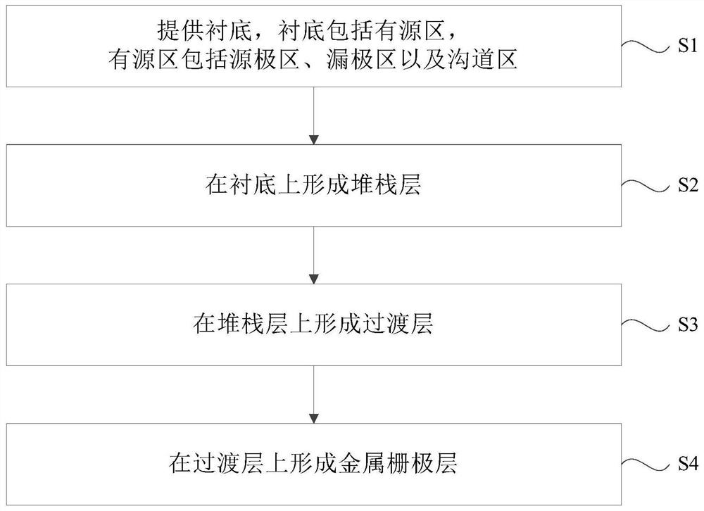
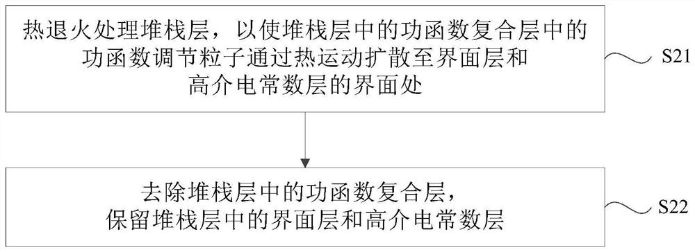
[0077] The inventor of the present application found in the actual research process that the current HKMG transistor structure includes a sequentially stacked substrate, a silicon oxide layer, a high dielectric constant dielectric layer, a work function adjustment layer and a metal gate. where the work function adjustment layer is La x O y (Al x O y ) layer and TiN layer composite layer, TiN layer is generally made by PVD method (Physical Vapor Deposition, physical vapor deposition), and LaO (AlO) layer is generally made by ALD method (Atomic layer deposition, atomic layer deposition), to Controls the thickness of the LaO(AlO) layer. However, the current PVD and ALD processes in different equipment are easy to cause, and the oxygen atoms in the LaO (AlO) prepared by ALD are easily diffused into the TiN layer, resulting in the formation of oxide TiO in the TiN layer, which makes the Al element or La Elements are more difficult to diffuse into the dielectric layer. And in t...


PUM


Abstract

The invention provides a manufacturing method of a semiconductor structure and the semiconductor structure, relates to the technical field of semiconductor manufacturing, and aims to solve the problems that a titanium nitride layer in a current work function adjustment layer is easy to oxidize, so that an interlayer resistance value is increased, and the performance of the semiconductor structure is influenced. The manufacturing method of the semiconductor structure comprises the steps of providing a substrate; forming a stack layer on the substrate; wherein the stack layer comprises an interface layer, a high dielectric constant layer and a work function composite layer which are stacked in sequence; forming a transition layer on the stack layer; and forming a metal gate layer on the transition layer. Wherein the work function composite layer is prepared through a physical vapor deposition method. According to the semiconductor structure and the manufacturing method thereof, the problem that part of materials in the used work function adjusting layer are prone to oxidation in the work function adjusting process can be effectively relieved, and therefore the interlayer resistance value in the semiconductor structure is reduced, the work function adjusting process can be completed easily, and the performance of the semiconductor structure is improved.

Description

technical field [0001] The present invention relates to the technical field of semiconductor manufacturing, and in particular, to a method for manufacturing a semiconductor structure and a semiconductor structure. Background technique [0002] A transistor is an important device in a dynamic random access memory (dynamic random access memory, DRAM for short), and the performance of the transistor affects the access performance of the DRAM device. [0003] As the size of transistors continues to shrink, HKMG (High-k and Metal Gate, high dielectric constant dielectric layer and metal gate) technology has become a common preparation method for transistor devices with feature sizes less than 45nm, which can improve the performance of transistors. switching speed, and reduce gate leakage current, thereby optimizing the access performance of DRAM devices. The transistor structure of HKMG includes a substrate, a silicon oxide layer, a high dielectric constant dielectric layer, a w...

Claims


Application Information

Patent Timeline
Patent Type & Authority Applications(China)
IPC IPC(8): H01L21/28H01L21/285H01L29/423H01L21/336H01L29/78H01L21/8242H01L27/108
CPCH01L21/28088H01L21/2855H01L29/42356H01L29/66477H01L29/78H10B12/30H10B12/05H01L29/423H01L21/28H01L21/285H01L29/66H01L27/092H01L27/088H10B12/00
Inventor 杨蒙蒙白杰
Owner CHANGXIN MEMORY TECH INC
Why Eureka
Try Eureka