Semiconductor device
a technology of semiconductor devices and semiconductors, applied in the direction of semiconductor devices, semiconductor/solid-state device details, electrical apparatus, etc., can solve the problems of reducing the insulation resistance, reducing the life affecting the performance of power semiconductor devices, etc., to achieve the effect of suppressing moisture from entering
- Summary
- Abstract
- Description
- Claims
- Application Information
AI Technical Summary
Benefits of technology
Problems solved by technology
Method used
Image


Examples
embodiment 1
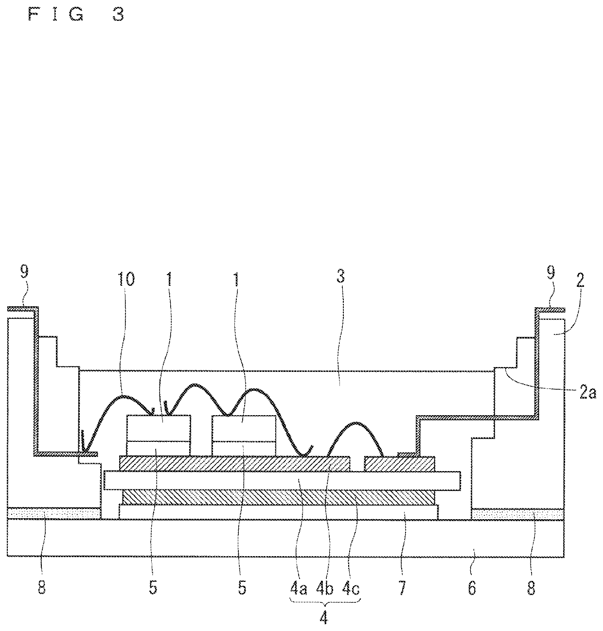
[0029]FIG. 1 is a schematic cross-sectional view of a semiconductor device 100 according to Embodiment 1. As illustrated in FIG. 1, the semiconductor device 100 is a power semiconductor device having a structure in which semiconductor elements 1 being power semiconductor elements are housed in a case 2 and sealed with a sealing material 3. Semiconductor elements 1 are Insulated Gate Bipolar Transistors (IGBT), Metal Oxide Semiconductor Field Effect Transistors (MOSFET) or the like formed of silicon (Si), silicon carbide (SiC), gallium nitride (GaN), or the like.
[0030]The semiconductor elements 1 are mounted on an insulating substrate 4, and the insulating substrate 4 is mounted on a base plate 6. The insulating substrate 4 is composed of an insulating layer 4a, a circuit pattern 4b formed on the upper surface of the insulating layer 4a, and a circuit pattern 4c formed on the lower surface of the insulating layer 4a. The semiconductor elements 1 are bonded to the circuit pattern 4b v...
embodiment 2
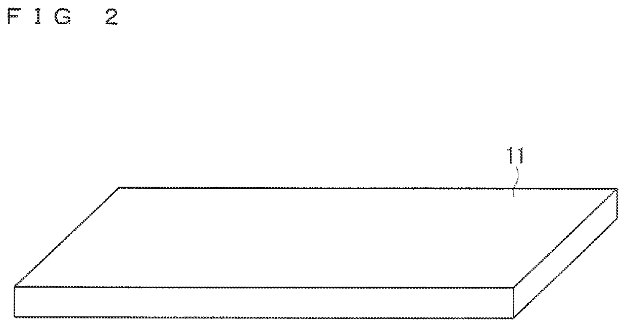
[0047]FIG. 7 is a schematic cross-sectional view of a semiconductor device according to Embodiment 2. FIG. 8 is a top view and a cross-sectional view of a low moisture permeable sheet 11 according to Embodiment 2. In Embodiment 2, a low moisture permeable sheet 11 has a convex portion 11a at a peripheral edge thereof, that is, a portion interposed between a case 2 and a lid 12, and the case 2 is provided with a groove 2b into which the convex portion 11a of the low moisture permeable sheet 11 is to be inserted.
[0048]Further, in Embodiment 2, the convex portion 11a is provided at the end portion of the low moisture permeability sheet 11; therefore, the end portion of the low moisture permeability sheet 11 is L-shaped in cross-sectional view (As illustrated in FIG. 8, the low moisture permeable sheet 11 is U-shaped when viewed in the entire cross section of the low moisture permeable sheet 11). Further, the groove 2b of the case 2 is provided in the counterbore portion 2a. Other confi...
embodiment 3
[0051]FIG. 9 is a schematic cross-sectional view of a semiconductor device 100 according to Embodiment 3. As illustrated in FIG. 9, in the semiconductor device 100 of Embodiment 3, a low moisture permeable sheet 14 (second low moisture permeable sheet) is provided at the adhesive interface between a case 2 and a base plate 6. The shape of the low moisture permeable sheet 14 is a frame shape in a plan view as illustrated in FIG. 10, and extends in the adhesive interface between the case 2 and the base plate 6 so as to surround a sealing material 3. The low moisture permeable material constituting the low moisture permeable sheet 14 may be the same as a low moisture permeable sheet 11 covering the sealing material 3, and the moisture permeability thereof is preferably 1 g / m2×24 Hr or less.
[0052]In order to prevent the semiconductor device 100 from being enlarged in size, the thickness of the low moisture permeable sheet 14 is preferably 3 mm or less, and more preferably 1 mm or less. ...
PUM
| Property | Measurement | Unit |
|---|---|---|
| humidity | aaaaa | aaaaa |
| temperature | aaaaa | aaaaa |
| thickness | aaaaa | aaaaa |
Abstract
Description
Claims
Application Information
 - Generate Ideas
- Intellectual Property
- Life Sciences
- Materials
- Tech Scout
- Unparalleled Data Quality
- Higher Quality Content
- 60% Fewer Hallucinations
Browse by: Latest US Patents, China's latest patents, Technical Efficacy Thesaurus, Application Domain, Technology Topic, Popular Technical Reports.
© 2025 PatSnap. All rights reserved.Legal|Privacy policy|Modern Slavery Act Transparency Statement|Sitemap|About US| Contact US: help@patsnap.com