
Composite substrate for electro-optical element

a technology of electro-optical elements and composite substrates, applied in the direction of metal layered products, instruments, chemistry apparatuses and processes, etc., can solve the problems of composite substrates that cannot be obtained, light propagation loss may occur, etc., and achieve excellent reliability, small light propagation loss, and significant suppression of peeling

Pending Publication Date: 2022-05-19
NGK INSULATORS LTD
View PDF0 Cites 0 Cited by
  • Summary
  • Abstract
  • Description
  • Claims
  • Application Information

AI Technical Summary

Benefits of technology

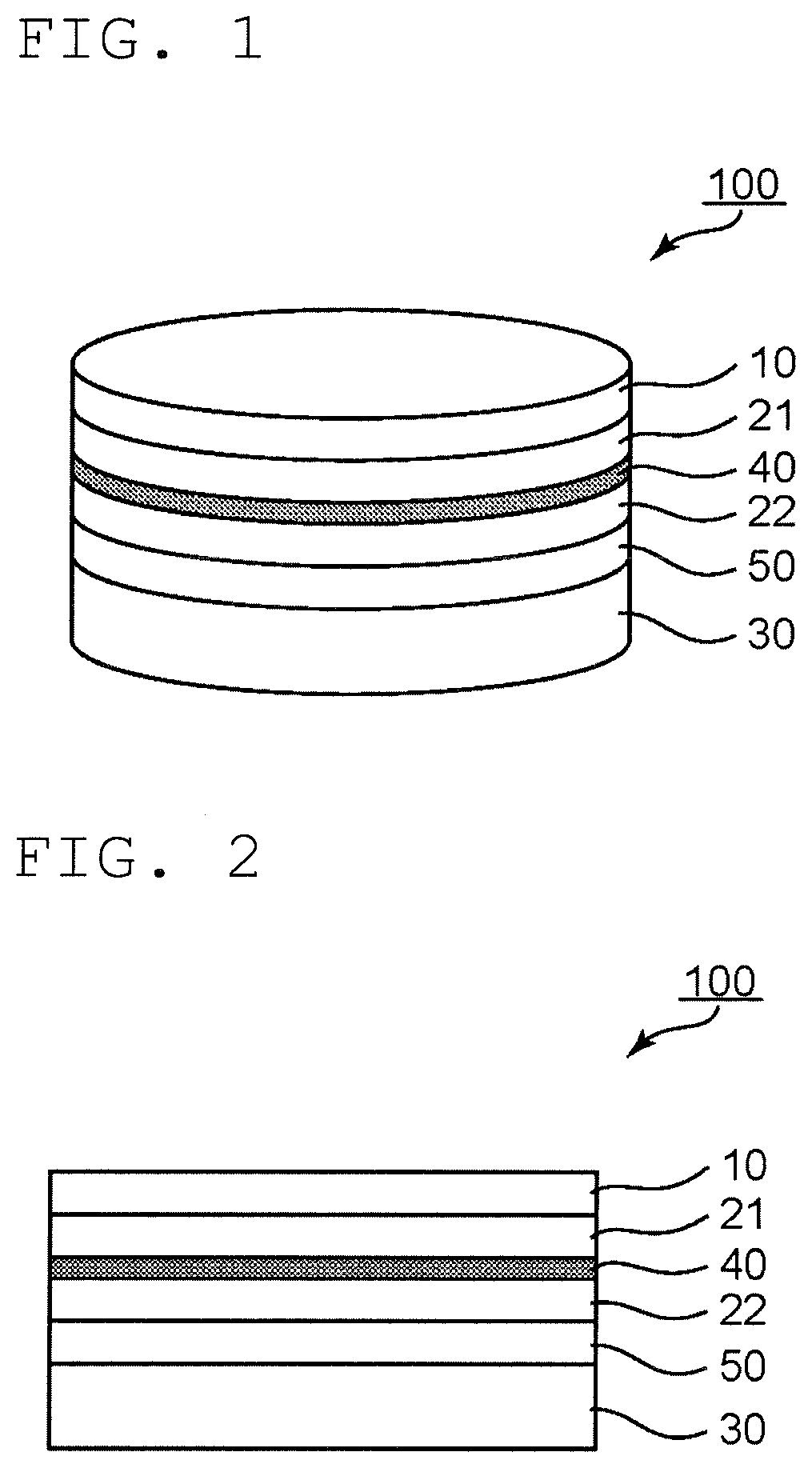
The present invention provides a composite substrate for an electro-optical element that integrates the electro-optical crystal substrate and the support substrate with two high dielectric layers directly joined to each other. This results in a composite substrate that reduces peeling and has low light propagation loss when used as an electro-optical element. The high-speed and low-voltage drive is possible. The support substrate or the low dielectric layer can be made of silicon oxide with a low argon concentration to achieve a thin electro-optical element with excellent reliability even under high-temperature environments. The thickness of the first high dielectric layer and the total thickness of the first and second high dielectric layers are set to predetermined values to make the electro-optical crystal substrate extremely thin while maintaining excellent effects.

Problems solved by technology

However, such a composite substrate has the following problems.
When the electro-optical crystal substrate and the thin film layer are directly joined to each other, light propagation loss may occur.
When the thin film layer and the support substrate are directly joined to each other, high-speed drive may be difficult, and depending on the situation, the joining itself may not be successful, with the result that a composite substrate may not be obtained.

Method used


Image

  • Composite substrate for electro-optical element
  • Composite substrate for electro-optical element

Examples


example 1

[0055]An X-cut lithium niobate substrate having a diameter of 4 inches was prepared as an electro-optical crystal substrate, and a silicon substrate having a diameter of 4 inches (thickness: 500 μm) was prepared as a support substrate. First, tantalum oxide was sputtered onto the electro-optical crystal substrate to form a first high dielectric layer having a thickness of 0.03 μm. Next, silicon oxide was sputtered onto the support substrate to form a low dielectric layer having a thickness of 10.0 μm. The obtained low dielectric layer was slightly subjected to CMP to reduce the arithmetic average roughness Ra on the surface of the low dielectric layer. Next, the surface of the low dielectric layer was washed, and tantalum oxide was sputtered onto the washed surface to form a second high dielectric layer having a thickness of 0.03 μm. Here, the arithmetic average roughness of the interface between the second high dielectric layer and the low dielectric layer and the arithmetic averag...

example 2

[0057]A composite substrate for an electro-optical element similar to that of FIG. 2 (provided that the low dielectric layer was not present between the second high dielectric layer and the support substrate) was obtained in the same manner as in Example 1 except that a quartz glass substrate (thickness: 500 μm) was used as the support substrate and a low dielectric layer was not formed on the support substrate. In the obtained composite substrate for an electro-optical element, no defects such as peeling were observed at the joining interface.

[0058]Further, an optical modulator was produced from the obtained composite substrate. The product Vπ·L of the half wavelength voltage Vπ and the electrode length L was 1.0 Vcm. The propagation loss of the optical waveguide was 0.5 dB. Further, the modulation band was 50 GHz, and no ripples were detected in modulation characteristics at a frequency equal to or less than this frequency.

example 17

[0069]An X-cut lithium niobate substrate having a diameter of 4 inches was prepared as an electro-optical crystal substrate, and a glass substrate having a diameter of 4 inches (thickness: 500 μm) was prepared as a support substrate. The support substrate (glass substrate) was formed by a sol-gel method to be highly purified. The argon ion concentration of the glass substrate was measured through use of energy dispersive X-ray analysis and found to be 1 atomic %. A composite substrate was produced through use of the electro-optical crystal substrate and the support substrate. Specifically, the composite substrate was produced as follows. First, tantalum oxide was sputtered onto each of the electro-optical crystal substrate and the glass substrate to form a first high dielectric layer and a second high dielectric layer each having a thickness of 0.03 μm. The argon concentrations of the formed first high dielectric layer and the formed second high dielectric layer were measured by ene...


PUM

PropertyMeasurementUnit
thicknessaaaaaaaaaa
thicknessaaaaaaaaaa
thicknessaaaaaaaaaa

Abstract

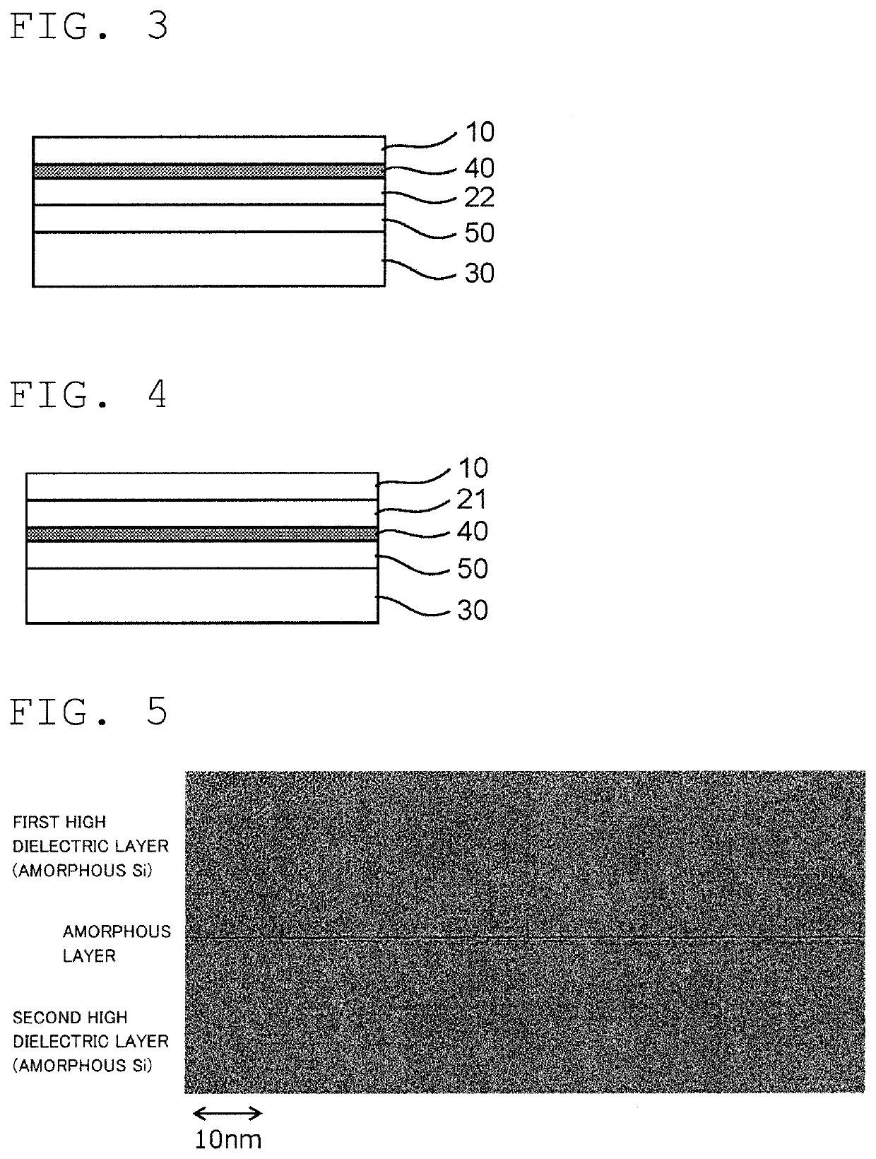
There is provided a composite substrate in which peeling is significantly suppressed, light propagation loss is small when used as an electro-optical element, and high-speed and low-voltage drive is possible, and which can achieve an extremely thin electro-optical element capable of maintaining excellent reliability even under a severe high-temperature environment. A composite substrate for an electro-optical element according to an embodiment of the present invention includes: an electro-optical crystal substrate having an electro-optical effect; a first high dielectric layer; a second high dielectric layer; and a support substrate in the stated order. The first high dielectric layer and the second high dielectric layer are directly joined to each other, and an amorphous layer is formed at a joining interface between the first high dielectric layer and the second high dielectric layer.

Description

TECHNICAL FIELD[0001]The present invention relates to a composite substrate for an electro-optical element.BACKGROUND ART[0002]Various electro-optical elements have been known. The electro-optical element can convert an electric signal into an optical signal through use of an electro-optical effect. The electro-optical element is adopted, for example, in optical and radio wave fusion communication, and the development thereof is underway in order to achieve high-speed and large-capacity communication, low power consumption (low drive voltage), and a low footprint. Because of this, for example, the adoption of a configuration of the electro-optical element using a composite substrate has started. As a composite substrate for an electro-optical element, there has been known a composite substrate in which an electro-optical crystal substrate having an electro-optical effect and a support substrate are integrated by direct joining through intermediation of a thin film layer (for example...

Claims


Application Information

Patent Timeline
Patent Type & Authority Applications(United States)
IPC IPC(8): G02F1/01
CPCG02F1/0118G02F1/0113G02F1/0305G02F1/0018G02F1/03B32B15/04G02F2202/09G02B6/12G02B2006/12142G02F1/035
Inventor HATTORI, RYOSUKETAI, TOMOYOSHIASAI, KEIICHIROKONDO, JUNGO
Owner NGK INSULATORS LTD
Learn More