Heterogeneously integrated photonic devices with improved optical coupling between waveguides

a waveguide and optical coupling technology, applied in the field of semiconductor processing, can solve the problems of increasing packaging costs, scaling limitations, and single material systems that do not provide complete functionality, and achieve the effect of facilitating efficient adiabatic transformation

Active Publication Date: 2022-04-21
NEXUS PHOTONICS INC
View PDF0 Cites 1 Cited by
  • Summary
  • Abstract
  • Description
  • Claims
  • Application Information

AI Technical Summary

Benefits of technology

[0010]In this embodiment, if the first optical mode differs from the second optical mode by more than a predetermined amount, a tapered waveguide structure in at least one of the second and third elements facilitates efficient adiabatic transformation between the first optical mode and the second optical mode. Mutual alignments of the first, second and third elements are defined using lithographic alignment marks.

Problems solved by technology

Often, a single material system does not provide complete functionality (low propagation loss, high or low confinement in the waveguide, electrically pumped optical gain, efficient modulation, etc.) or parts of that functionality provide sub-optimal performance.
Such an approach is challenging due to a need for very fine alignment, which increases packaging costs and introduces scaling limitations.
Standard heterogeneous integration is very powerful, but might be challenging in some materials combinations due to a variety of reasons including small native wafers (limiting the total available material, as in e.g. native GaN), problems related to bonding surface quality (e.g. thick buffer layer growth resulting in increased surface roughness), problems relating to substrate removal (e.g. absence of appropriately selective etches) and / or others.
A second limitation of standard heterogeneous integration arises from a limitation in the smallest feature size that can readily be fabricated.
In cases where there is a larger difference in effective indices, such as between e.g. SiN and GaAs, the requirements on taper tip dimensions become prohibitive, limiting efficient power transfer.
Achieving such dimensions is complex and may be cost prohibitive.

Method used


Image

  • Heterogeneously integrated photonic devices with improved optical coupling between waveguides
  • Heterogeneously integrated photonic devices with improved optical coupling between waveguides
  • Heterogeneously integrated photonic devices with improved optical coupling between waveguides

Examples


Embodiment Construction

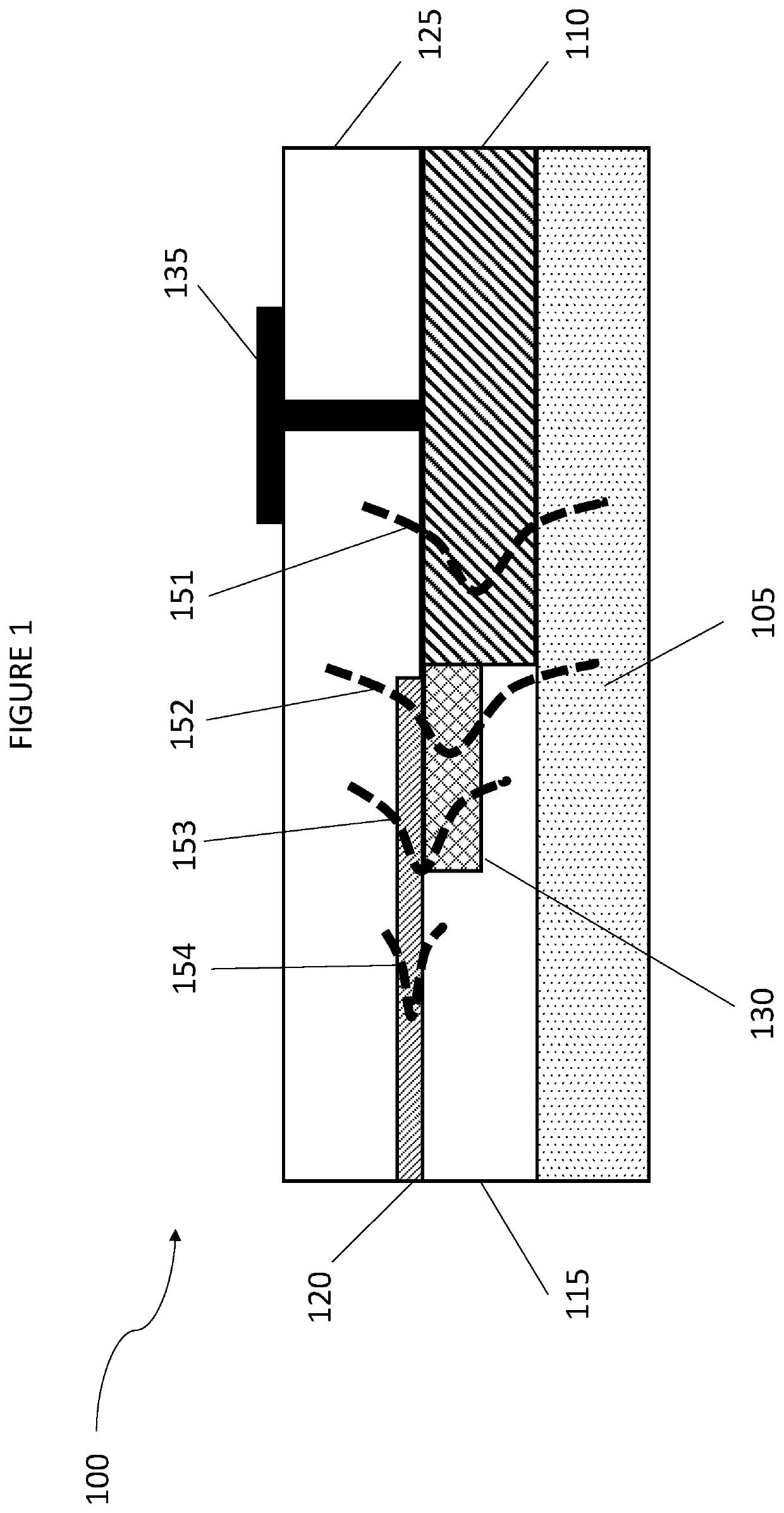
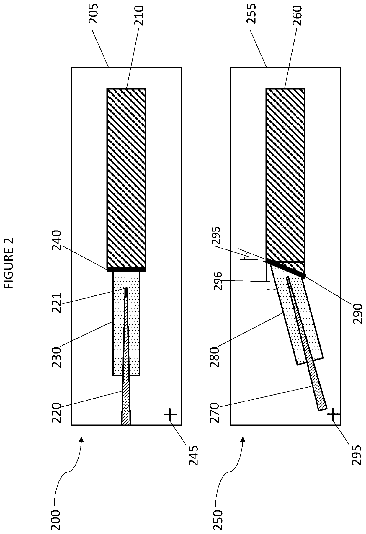
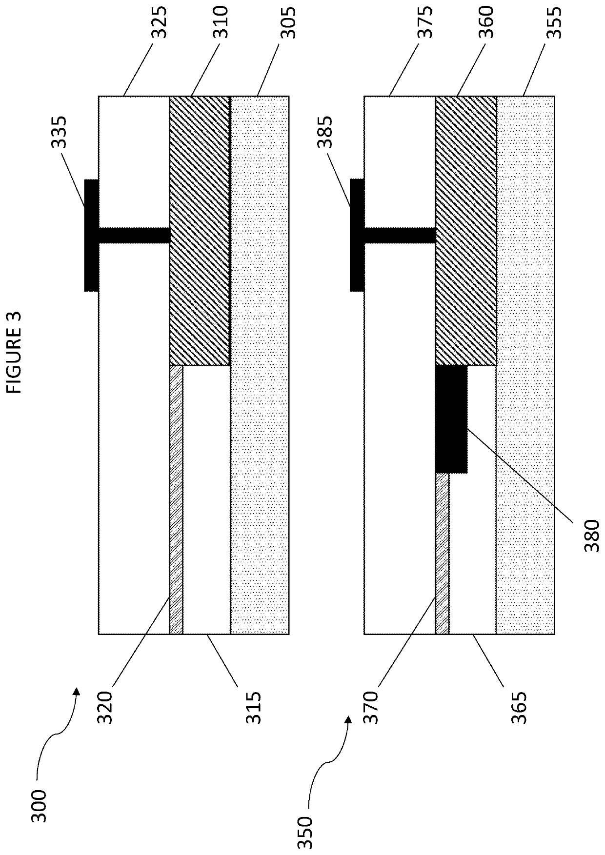
[0017]Described herein include embodiments of a method and system for realization of photonic integrated circuits using epitaxial growth, wafer bonding and / or deposition of dissimilar materials where optical coupling is improved by use of mode conversion and a butt-coupling scheme.

[0018]In the following detailed description, reference is made to the accompanying drawings which form a part hereof, wherein like numerals designate like parts throughout, and in which are shown by way of illustration embodiments in which the subject matter of the present disclosure may be practiced. It is to be understood that other embodiments may be utilized and structural or logical changes may be made without departing from the scope of the present disclosure. Therefore, the following detailed description is not to be taken in a limiting sense, and the scope of embodiments is defined by the appended claims and their equivalents.

[0019]The description may use perspective-based descriptions such as top / ...


PUM

PropertyMeasurementUnit
RMS roughnessaaaaaaaaaa
angleaaaaaaaaaa
angleaaaaaaaaaa

Abstract

An optical device comprises first, second and third elements fabricated on a common substrate. The first element comprises an active waveguide structure supporting a first optical mode, the second element, fabricated on a planarized top surface of the first element, comprises a passive waveguide structure supporting a second optical mode, and the third element, at least partly butt-coupled to the first element, comprises an intermediate waveguide structure, positioned such that a top surface of the intermediate structure underlies a bottom surface of the passive waveguide structure. If the first optical mode differs from the second optical mode by more than a predetermined amount, a tapered waveguide structure in at least one of the second and third elements facilitates efficient adiabatic transformation between the first optical mode and the second optical mode. Mutual alignments of the first, second and third elements are defined using lithographic alignment marks.

Description

FIELD OF THE INVENTION[0001]The present invention relates to semiconductor processing. More specifically, certain embodiments of the invention relate to a method and system for realization of photonic integrated circuits using dissimilar materials that are optically coupled.BACKGROUND OF THE INVENTION[0002]A photonic integrated circuit (PIC) or integrated optical circuit is a device that integrates multiple photonic functions and as such is analogous to an electronic integrated circuit. The major difference between the two is that a photonic integrated circuit provides functions for information signals imposed on optical carrier waves.[0003]PICs can be realized in a number of material systems, generally determined by the wavelength of operation, such as those based on indium phosphide (InP), gallium arsenide (GaAs), or gallium nitride (GaN) which are direct bandgap materials capable of efficient light generation. Other PICs can be realized by indirect bandgap materials such as e.g. ...

Claims


Application Information

Patent Timeline
Patent Type & Authority Applications(United States)
IPC IPC(8): G02B6/14G02B6/13G02B6/12G02B6/122G02B6/132
CPCG02B6/14G02B6/131G02B6/12004G02B2006/1209G02B6/132G02B2006/12152G02B6/1228G02B2006/12147G02B2006/1204
Inventor ZHANG, CHONGPARK, HYUN DAITRAN, MINHKOMLJENOVIC, TIN
Owner NEXUS PHOTONICS INC
Why Eureka
Try Eureka