
ESD protection device with low trigger voltage

Active Publication Date: 2021-03-04
CHANG WEN TSUNG
View PDF0 Cites 1 Cited by
  • Summary
  • Abstract
  • Description
  • Claims
  • Application Information

AI Technical Summary

Benefits of technology

The present patent introduces a device structure that uses parasitic NPN and PNP transistors to form a SCR device for ESD protection. This results in a snapback characteristic that improves the device's ability to drain current and reduce clamping voltage. The structural restrictions of the device are also loosened, allowing for the formation of a low-capacitance ESD protection device on a single wafer. This is done through modifying the fabrication process for low-capacitance diodes.

Problems solved by technology

Process conditions for N+P+P−N+ are considerably constrained—it is difficult to fabricate low-capacitance diodes on the same wafer.

Method used


Image

  • ESD protection device with low trigger voltage
  • ESD protection device with low trigger voltage
  • ESD protection device with low trigger voltage

Examples


Embodiment Construction

[0035]The objects, advantages and features of the present invention will become apparent from the following detailed descriptions of the embodiments in conjunction with the accompanying drawings.

[0036]In the following description, numerous specific details are set forth to provide a thorough understanding of the presented embodiments. However, the disclosed embodiments may be implemented without some or all of these specific details. In other instances, conventional structures and operations have not been described in detail to not unnecessarily obscure the disclosed embodiments. It should be understood that the various embodiments shown in the drawings are schematic, and are not necessarily drawn to scale.

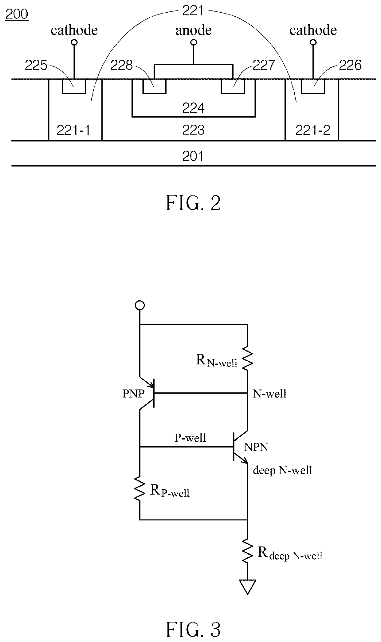
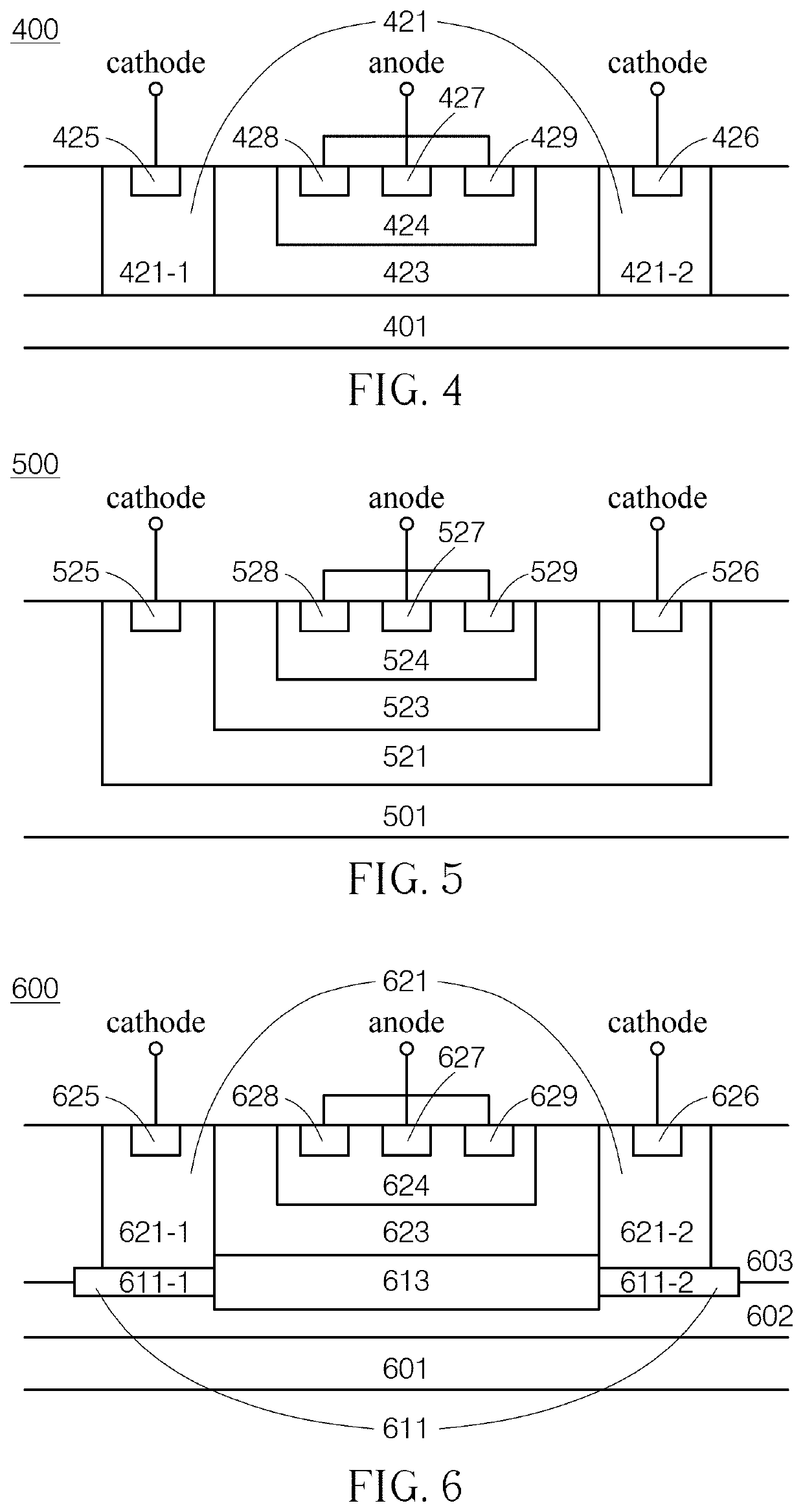
[0037]FIG. 2 is a cross-sectional diagram of a semiconductor structure of an ESD protection device 200 according to one embodiment of the present invention. As shown in FIG. 2, the ESD protection device 200 includes an N-type substrate 201. A P-well 223 and a deep N-well 221 are f...


PUM


Abstract

The present invention provides an ESD protection device with the mechanism of punch through to achieve low trigger voltage. At the same time, the structure of ESD protection device includes parasitic NPN and parasitic PNP. Parasitic NPN and parasitic PNP will form a silicon controlled rectifier (SCR) device with snapback behavior to increase the protection capability of ESD protection device.

Description

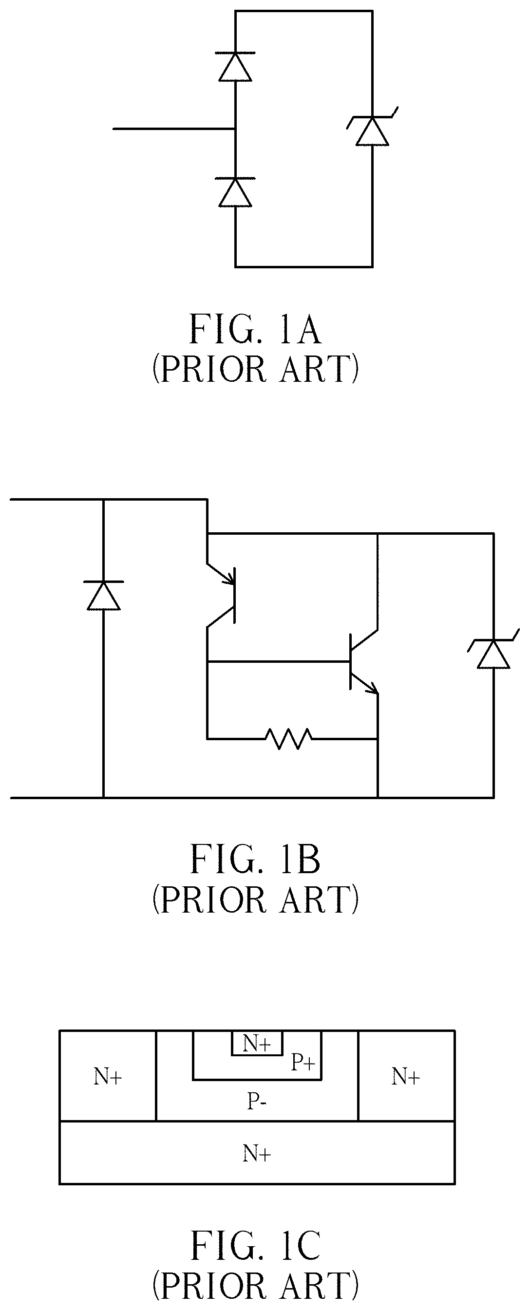
CROSS-REFERENCE TO RELATED APPLICATIONS[0001]The present application is related to and claims priority to Taiwan Patent Application No. 108131780 filed on Sep. 4, 2019, which is hereby incorporated by reference in its entirety.BACKGROUND OF THE INVENTIONTechnical Field[0002]The present invention relates to electrostatic discharge (ESD) protection devices, structures thereof, and methods of forming the semiconductor devices.Description of the Prior Art[0003]Electrostatic discharge (ESD) protection devices are required at the inputs and outputs of a circuit. The electrostatic discharge protection devices have good capability to drain a current to ground, thereby protecting the circuit from the damage of electrostatic discharge, lightning strikes, surges, or the like. Conventionally, different methods and structures have been utilized to form the ESD protection devices in the semiconductor industry.[0004]One common ESD protection technology uses a Zener diode as a main device, as shown...

Claims


Application Information

Patent Timeline
IPC IPC(8): H01L27/02
CPCH01L27/0262H01L29/0603H01L29/7424H01L29/87
Inventor CHANG, WEN-TSUNG
Owner CHANG WEN TSUNG
Learn More