
Blue-emitting nanocrystals with cubic shape and fluoride passivation

a nanocrystal and fluoride technology, applied in the field of nanotechnology, can solve the problems of insufficient ligand coverage on the surface, pits and kinks of rounded particle surfaces, difficult to passivate with ligands, and rise in operating voltage and irreversible electrochemical degradation

Active Publication Date: 2021-01-14
SHOEI CHEM IND CO LTD
View PDF0 Cites 4 Cited by
  • Summary
  • Abstract
  • Description
  • Claims
  • Application Information

AI Technical Summary

Benefits of technology

The patent text is stating that the time it takes for an electroluminescent device to reach 50% of its initial brightness is at least three times longer when certain fluorides are not present in the device. The technical effect of this is that the device takes longer to reach its maximum brightness, which may be helpful in certain applications where longer lifetimes are desired.

Problems solved by technology

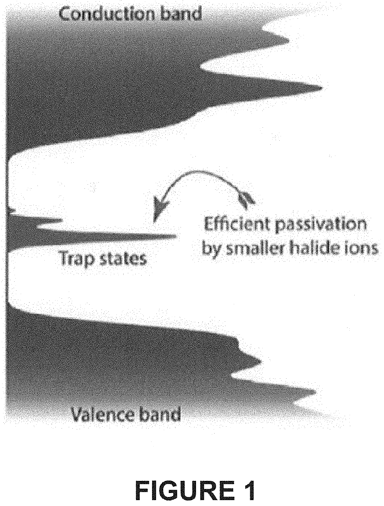
Steric bulk of long-chain alkyl ligands can result in insufficient ligand coverage on the surface of semiconductor nanocrystals due to packing limitation.
Similarly, rounded particle surfaces exhibit steps, pits, and kinks that can be difficult to passivate with ligands.
Holes will accumulate at the HTL-QD interface leading to a rise in operating voltage and irreversible electrochemical degradation.
The native ligand set (e.g., carboxylates and phosphines) of most quantum dots is hydrophobic and thus quantum dots comprising these native ligands are not soluble in a wide range of organic media and are incompatible with matrix materials commonly used in the preparation of quantum dots films.

Method used


Image

  • Blue-emitting nanocrystals with cubic shape and fluoride passivation
  • Blue-emitting nanocrystals with cubic shape and fluoride passivation
  • Blue-emitting nanocrystals with cubic shape and fluoride passivation

Examples


example 1

[0370]Synthesis of ZnSe1-xTex Alloy Nanocrystals Using TOPTe Precursor

[0371]Preparation of TOPTe precursor: the Te precursor mixture was prepared by first diluting trioctylphosphine telluride (1 M Te, 230 μL) with 2.5 mL dried and distilled oleylamine. Lithium triethylborohydride (1 M in THF, 230 μL) was added to this solution which resulted in a deeply purple solution. Finally, zinc oleate (0.5 M in trioctylphosphine (TOP), 460 μL) was added which resulted in a colorless opaque viscous gel which could be drawn into a syringe.

[0372]Oleylamine (15 mL) was added to a 100 mL three neck flask and degassed under vacuum at 110° C. for 30 minutes. Then the mixture was heated to 300° C. under nitrogen flow. Once this temperature was reached, a solution of trioctylphosphine selenide (TOPSe, 2.7 mmol) and diphenylphosphine (225 μL) in TOP (2.9 mL total) was added to the flask. Once the temperature rebounded to 300° C., the TOPTe precursor described above and a solution of diethyl zinc (295 μL...

example 2

Synthesis of ZnSe Nanocrystals

[0373]ZnSe nanocrystals were prepared using the method of Example 1 without the injection of the TOPTe precursor.

example 3

[0374]Synthesis of ZnSe1-xTex / ZnSe Buffered Nanocrystals

[0375]A ZnSe buffer layer on ZnSe1-xTex nanocrystals of 4.0 nm average diameter with a target shell thickness of 4 monolayers (ML) ZnSe was prepared.

[0376]A 100 mL three neck flask was charged with zinc oleate (6.23 g), lauric acid (3.96 g), trioctylphosphine oxide (4.66 g), and TOP (9.4 mL). The flask was subjected to three vacuum and nitrogen backfill cycles before heating to 100° C. and degassing for 30 minutes. The reaction mixture was placed under a blanket of nitrogen and a solution of ZnSe1-xTex cores (4.0 mL, 28.0 mg / mL in hexane) mixed with TOPSe (1.8 mL of 0.3 M selenium in TOP) was added to the flask. The flask was evacuated for 2 minutes and then heated to 310° C. under nitrogen flow. Once this temperature was reached, the slow infusion of TOPSe (10.4 mL, 0.3 M in TOP) with a rate of 0.325 mL / min was started. After the selenium infusion was finished, the reaction was held at 310° C. for 10 minutes and then cooled to...


PUM

PropertyMeasurementUnit
molar ratioaaaaaaaaaa
photoluminescence quantum yieldaaaaaaaaaa

Abstract

This disclosure pertains to the field of nanotechnology. The disclosure provides methods of preparing nanostructures with fluoride passivation. The disclosure also provides methods of preparing nanostructures with fluoride and amine passivation. The nanostructures have high quantum yield, narrow emission peak width, tunable emission wavelength, and colloidal stability. Also provided are nanostructures prepared using the methods. And, nanostructure films and molded articles comprising the nanostructures are also provided.

Description

FIELD OF THE INVENTIONField of the Invention[0001]This disclosure pertains to the field of nanotechnology. The disclosure provides methods of preparing nanostructures with fluoride passivation. The disclosure also provides methods of preparing nanostructures with fluoride and amine passivation. The nanostructures have high quantum yield, narrow emission peak width, tunable emission wavelength, and colloidal stability. Also provided are nanostructures prepared using the methods. And, nanostructure films and molded articles comprising the nanostructures are also provided.Background Art[0002]Semiconductor nanostructures can be incorporated into a variety of electronic and optical devices. The electrical and optical properties of such nanostructures vary, e.g., depending on their composition, shape, and size. For example, size-tunable properties of semiconductor nanoparticles are of great interest for applications such as light emitting diodes (LEDs) and liquid crystal displays (LCDs). ...

Claims


Application Information

Patent Timeline
Patent Type & Authority Applications(United States)
IPC IPC(8): C09K11/88C09K11/08C09K11/02
CPCC09K11/883C09K11/02C09K11/0883C09K11/56C09K11/70C09K11/612C09K11/025B82Y30/00B82Y40/00C08J5/18C08K9/04C08K9/02
Inventor NEWMEYER, BENJAMINIPPEN, CHRISTIANMA, RUIQINGBARRERA, DIEGOMANDERS, JESSE ROBERT
Owner SHOEI CHEM IND CO LTD
Learn More