Flexible display
a flexible display and display panel technology, applied in non-linear optics, instruments, organic semiconductor devices, etc., can solve the problems of easy breakage of parts of film layers, failure of flexible display panels, etc., and achieve good bending tolerance
- Summary
- Abstract
- Description
- Claims
- Application Information
AI Technical Summary
Benefits of technology
Problems solved by technology
Method used
Image

Examples
first embodiment
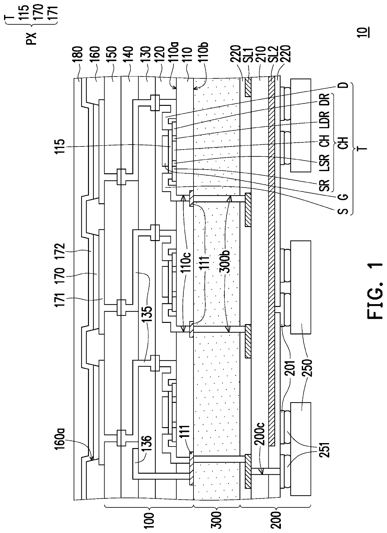
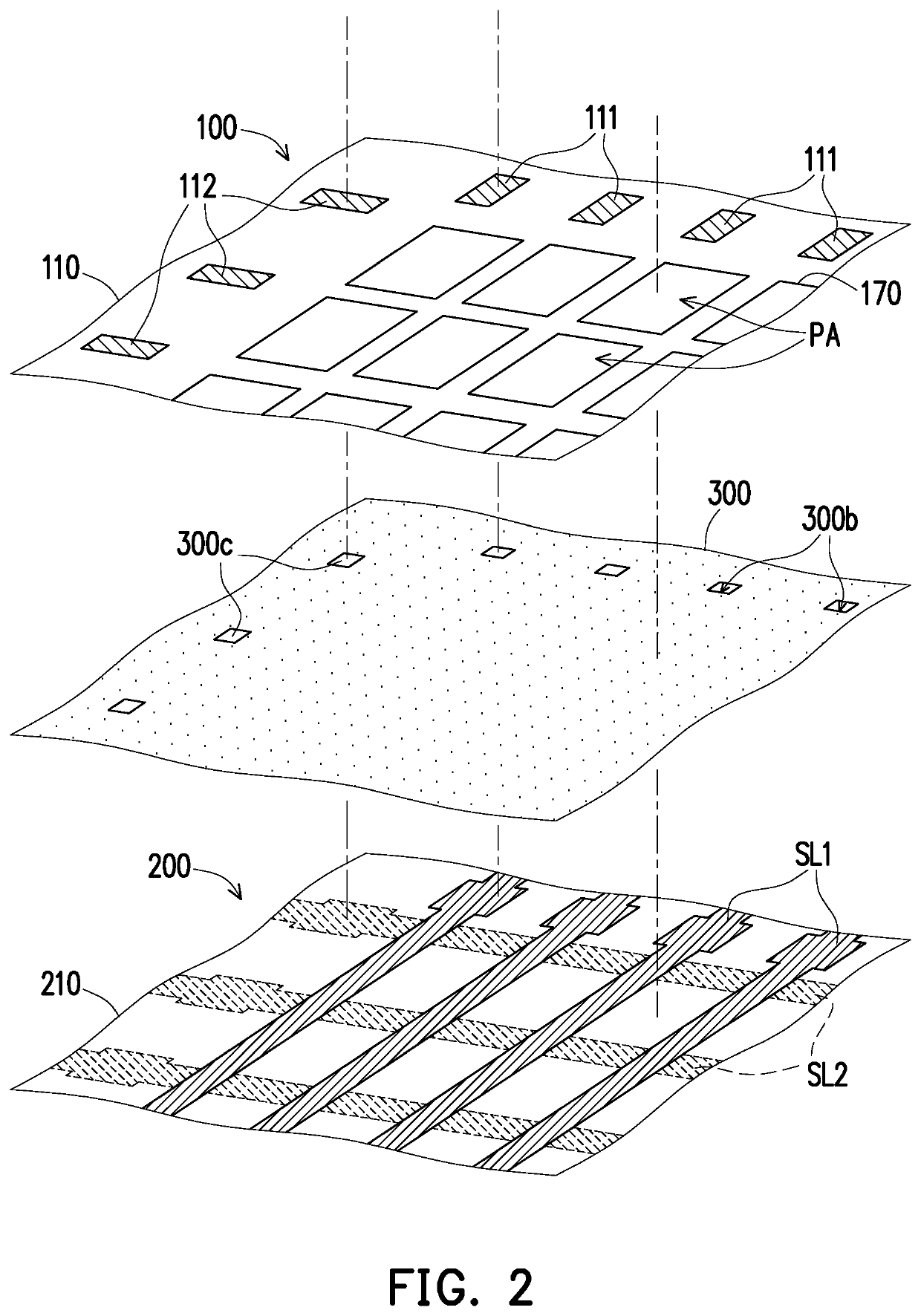
[0032]FIG. 1 is a schematic cross-sectional view of a flexible display according to the disclosure. FIG. 2 is a schematic top view of the flexible circuit board, the adhesive layer, and the pixel circuit layer of FIG. 1. It should be noted that, for a clear presentation, the flexible circuit board 200 of FIG. 2 omits the illustration of the protective layer 220, the fourth conductive through holes 200c, the conductors 251 and the driving chips 250 of FIG. 1, and the pixel circuit layer 100 of FIG. 2 only shows the buffer layer 110, the light emitting patterns 170, the first pads 111, and the second pads 112 of FIG. 1.
[0033]In the embodiment, a flexible display 10 may be a self-emitting display, and the self-emitting display includes, for example, an organic light emitting diode (OLED) display, a micro light emitting diode (micro-LED) display, or a mini light emitting diode (mini-LED) display. However, in other embodiments, the flexible display may also be a non-self-emitting display...
second embodiment
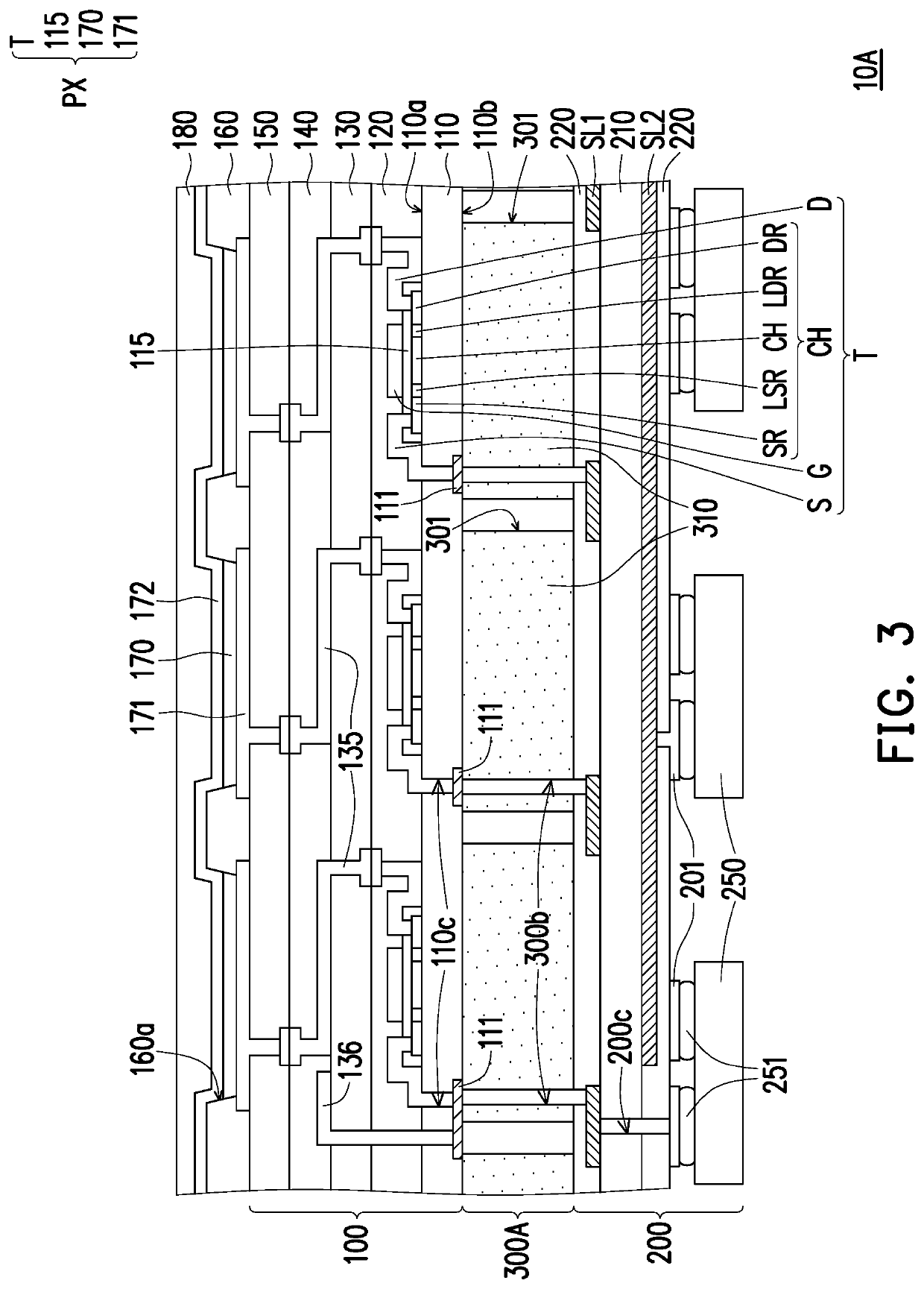
[0050]FIG. 3 is a schematic cross-sectional view of a flexible display according to the disclosure. FIG. 4 is a schematic top view of the flexible circuit board, the adhesive layer, and the pixel circuit layer of FIG. 3. It should be noted that, for a clear presentation, the flexible circuit board 200 of FIG. 4 omits the illustration of the protective layer 220, the fourth conductive through holes 200c, the conductors 251 and the driving chips 250 of FIG. 3, and the pixel circuit layer 100 of FIG. 4 only shows the buffer layer 110, the light emitting patterns 170, the first pads 111, and the second pads 112 of FIG. 3.
[0051]With reference to FIGS. 3 and 4, the difference between a flexible display 10A of this embodiment and the flexible display 10 of the previous embodiment lies in the structural design and disposition of an adhesive layer 300A of the flexible display 10A. Specifically, the adhesive layer 300A of the flexible display 10A has a plurality of first grooves 301, and an o...
third embodiment
[0053]FIG. 5 is a schematic cross-sectional view of a flexible display according to the disclosure. FIG. 6 is a schematic top view of the protective layer, the flexible circuit board, and the pixel circuit layer of FIG. 5. It should be noted that, for a clear presentation, the flexible circuit board 200 of FIG. 6 omits the illustration of the protective layer 220 of FIG. 5, and the pixel circuit layer 100 of FIG. 6 only shows the buffer layer 110, the light emitting patterns 170, the first pads 111, and the second pads 112 of FIG. 5.
[0054]With reference to FIGS. 5 and 6, the difference between a flexible display 10B of this embodiment and the flexible display 10 of the previous embodiment lies in that the flexible display 10B further includes a protective layer 190. In the embodiment, the protective layer 190 is disposed on a side of the flexible circuit board 200 away from the adhesive layer 300; that is, the flexible circuit board 200 is located between the adhesive layer 300 and ...
PUM
| Property | Measurement | Unit |
|---|---|---|
| crushing stress | aaaaa | aaaaa |
| anisotropic conductive | aaaaa | aaaaa |
| conductive | aaaaa | aaaaa |
Abstract
Description
Claims
Application Information
 - R&D
- Intellectual Property
- Life Sciences
- Materials
- Tech Scout
- Unparalleled Data Quality
- Higher Quality Content
- 60% Fewer Hallucinations
Browse by: Latest US Patents, China's latest patents, Technical Efficacy Thesaurus, Application Domain, Technology Topic, Popular Technical Reports.
© 2025 PatSnap. All rights reserved.Legal|Privacy policy|Modern Slavery Act Transparency Statement|Sitemap|About US| Contact US: help@patsnap.com