Active device substrate

a technology of active devices and substrates, applied in the field of active device substrates, can solve problems such as failure of flexible display panels, and achieve the effects of not easily cracked, good bending tolerance, and easy bending

Active Publication Date: 2021-07-20
AU OPTRONICS CORP
View PDF15 Cites 2 Cited by
  • Summary
  • Abstract
  • Description
  • Claims
  • Application Information

AI Technical Summary

Benefits of technology

[0005]The disclosure provides an active device substrate, which has good bending tolerance.
[0026]Based on the above, the active device substrate in the embodiment of the disclosure is provided with the organic insulation pattern in the first groove of the bending region. The peripheral wiring is disposed on the organic insulation pattern to cross the bending region and is extended from the active region to the peripheral region. Since the material of the organic insulation pattern is softer and not easily cracked due to bending, when the bending region is bent, the peripheral wiring is not easily affected by the organic insulation pattern to be cracked, and thus the active device substrate has good bending tolerance.

Problems solved by technology

When the flexible display panel is bent, the fragile inorganic insulation layer is easily cracked, which causes adjacent layer (e.g., first conductive layer, second conductive layer, etc.) to be cracked, thus leading to failure of flexible display panel.

Method used


Image

  • Active device substrate
  • Active device substrate
  • Active device substrate

Examples


Embodiment Construction

[0034]In order to make the disclosure more comprehensible, embodiments are described below as the examples to prove that the disclosure can actually be realized. In addition, wherever possible, the same reference numerals in drawings and embodiments represent the same or similar parts.

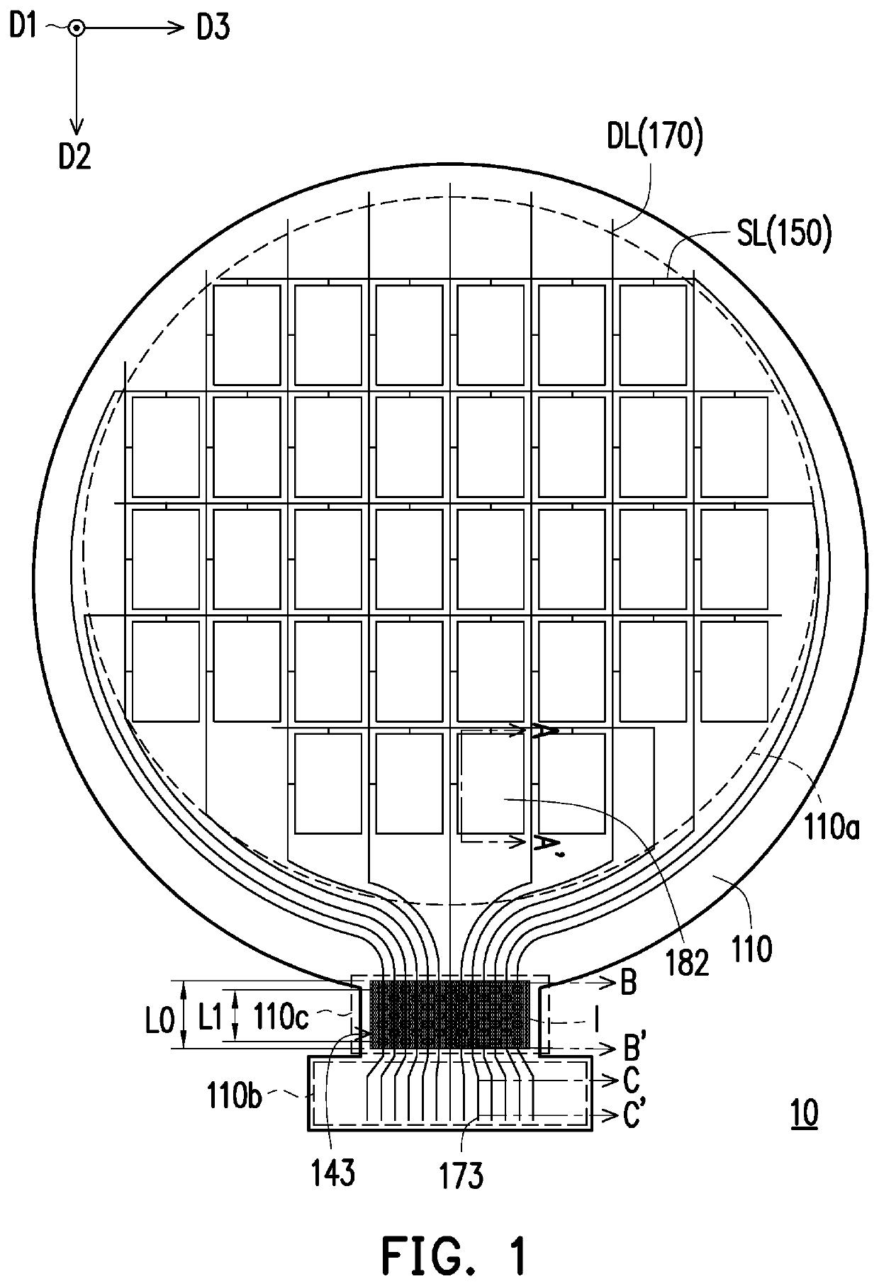
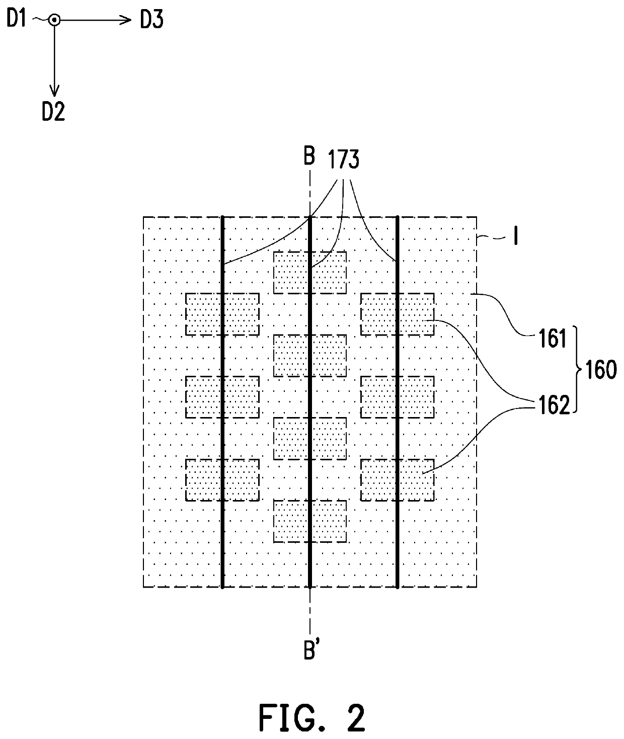
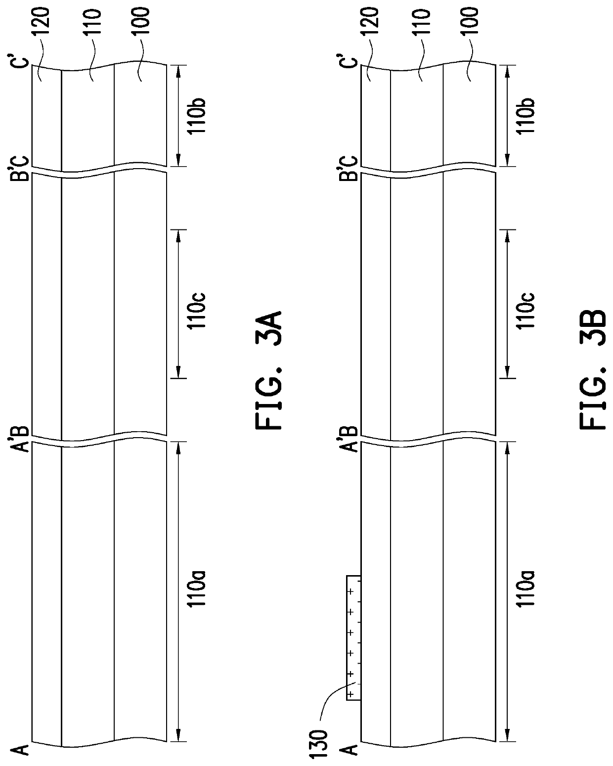
[0035]FIG. 1 is a schematic top view of an active device substrate 10 according to an embodiment of the disclosure. FIG. 2 is an enlarged schematic top view of a portion I of a bending region 110c of the active device substrate 10 in FIG. 1. FIG. 3A to FIG. 3Q are schematic cross-sectional views of a manufacturing process of an active device substrate according to an embodiment of the disclosure. Specifically, FIG. 3Q respectively corresponds to sectional lines A-A′, B-B′ and C-C′ taken along FIG. 1, and FIG. 1 omits illustration of a pixel defining layer 190, a light emitting layer 192 and a conductive device 153 in FIG. 3Q. FIG. 1, FIG. 2 and FIG. 3A-FIG. 3Q are illustrated to describe the manufactur...


PUM

PropertyMeasurementUnit
angleaaaaaaaaaa
angleaaaaaaaaaa
thicknessaaaaaaaaaa

Abstract

An active device substrate including a flexible substrate, an inorganic insulation layer, an organic insulation pattern, a conductive device and a peripheral wiring is provided. The flexible substrate has an active region, a peripheral region outside the active region and a bending region connected between the active region and the peripheral region. The inorganic insulation layer is disposed on the flexible substrate and has a groove disposed in the bending region. The organic insulation pattern is disposed in the groove of the inorganic insulation layer. The peripheral wiring is extended from the active region to the conductive device in the peripheral region. The peripheral wiring is disposed on the organic insulation pattern, and the organic insulation pattern is located between the peripheral wiring and the flexible substrate.

Description

CROSS REFERENCE TO RELATED APPLICATION[0001]This application claims the priority benefit of Taiwan application serial no. 107123668, filed on Jul. 9, 2018. The entirety of the above-mentioned patent application is hereby incorporated by reference herein and made a part of specification.BACKGROUNDField of the Disclosure[0002]The disclosure is related to a device substrate, and particularly to an active device substrate.Description of Related Art[0003]Along with advancement of display technologies, the application of display panel is expanded. For example, in early stage, display panel mainly serves as the screen of electronic devices (e.g., TV, computer, cell phone, etc.), and display panels applied to electronic device are mostly rigid display panels. Lately, some manufacturers apply display panel to wearable devices (e.g., watch, clothing, etc.), and display panels applied to wearable devices are mostly flexible display panels.[0004]Flexible display panel needs to be bendable to a ...

Claims


Application Information

Patent Timeline
Patent Type & Authority Patents(United States)
IPC IPC(8): H01L51/00H01L27/32
CPCH01L51/0097H01L27/3246H01L27/3258H01L27/3262H01L27/3276H01L2227/323H01L2251/5338H01L2251/558H01L23/562H01L27/1218Y02E10/549Y02P70/50H10K59/124H10K59/131H10K77/111H10K59/1201H10K2102/311H10K59/122H10K59/1213H10K2102/351
Inventor WANG, PEI-YUNCHEN, CHIA-KAI
Owner AU OPTRONICS CORP
Why Eureka
Try Eureka