Display apparatus

a display device and display technology, applied in the field of electronic devices, can solve the problems of increasing manufacturing difficulties and production costs under the stack layer structure adopted by a driving circuit design, and achieve the effect of easy manufacturing

Active Publication Date: 2021-08-10
AU OPTRONICS CORP
View PDF19 Cites 0 Cited by
  • Summary
  • Abstract
  • Description
  • Claims
  • Application Information

AI Technical Summary

Benefits of technology

[0005]The disclosure provides a display apparatus, which may be manufactured easily.
[0019]The disclosure provides a display apparatus having a touch function and a good bending tolerance.

Problems solved by technology

However, using a method of the stack layer structure would inevitably increase manufacturing difficulties and production costs.
Therefore, how to decrease the manufacturing difficulties and the production costs under the stack layer structure adopted by a design of the driving circuit is an important issue.

Method used


Image

  • Display apparatus
  • Display apparatus
  • Display apparatus

Examples


first embodiment

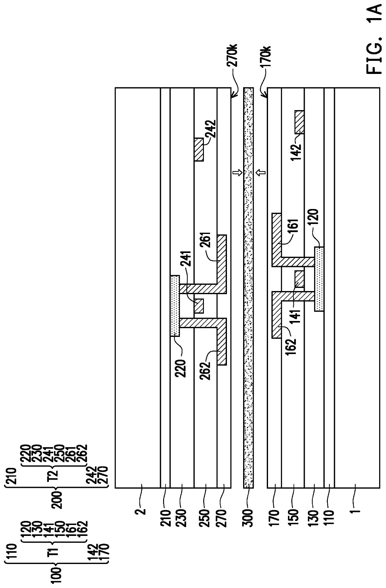
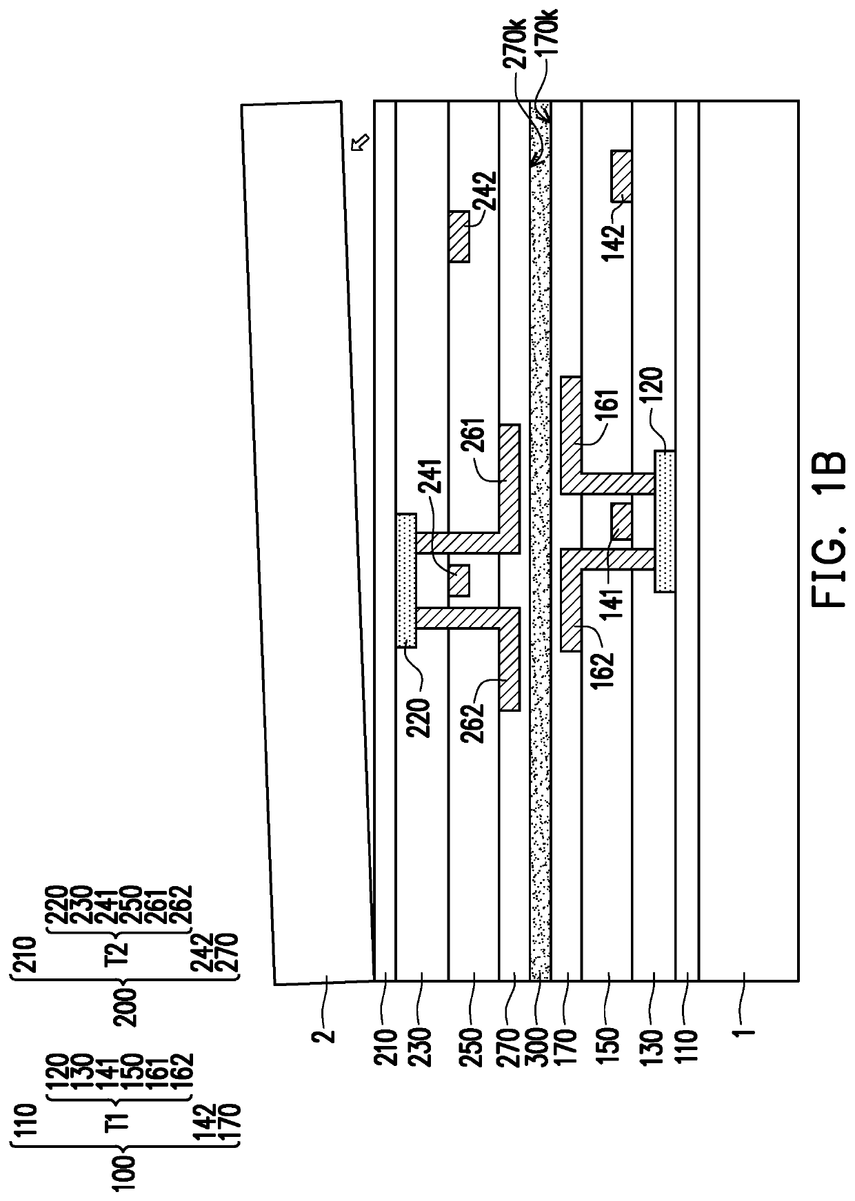
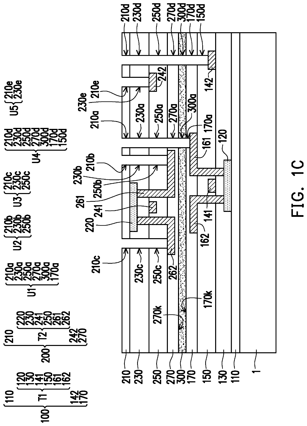
[0042]FIG. 1A-FIG. 1E are sectional schematic views of a manufacturing process of a display apparatus of the disclosure.

[0043]Please refer to FIG. 1A. Firstly, a first circuit substrate and a second circuit substrate are provided. The first circuit substrate includes a substrate 1 and a first circuit layer 100 disposed on the substrate 1. The second circuit substrate includes a substrate 2 and a second circuit layer 200 disposed on the substrate 2.

[0044]In the present embodiment, the first circuit layer 100 may include a thin-film transistor T1. The thin-film transistor T1 includes a semiconductor pattern 120, an insulating sublayer 130, a gate 141, a first electrode 161 and a second electrode 162. The insulating sublayer 130 is disposed between the gate 141 and the semiconductor pattern 120. A first electrode 161 and a second electrode 162 are electrically connected to two different areas of the semiconductor pattern 120 respectively.

[0045]In the present embodiment, the thin-film t...

second embodiment

[0079]FIG. 2 is a sectional schematic view of a display apparatus of the disclosure. A display apparatus 10A of FIG. 2 is similar to the display apparatus 10 of FIG. 1E. The difference of the two apparatuses lies in that the surface 170k of the first circuit layer 100 of the display apparatus 10A and the surface 270k of the second circuit layer 200 of the display apparatus 10A both face upward.

third embodiment

[0080]FIG. 3 is a sectional schematic view of a display apparatus of the disclosure. A display apparatus 10B of FIG. 3 is similar to the display apparatus 10 of FIG. 1E. The difference of the two apparatuses lies in that the surface 170k of the insulating sublayer 170 of the first circuit layer 100 of the display apparatus 10B and the surface 270k of the insulating sublayer 270 of the second circuit layer 200 of the display apparatus 10B both face downward.


PUM

PropertyMeasurementUnit
conductiveaaaaaaaaaa
insulatingaaaaaaaaaa
electroluminescentaaaaaaaaaa

Abstract

A display apparatus includes a substrate, a first circuit layer, a first adhesive layer, a second circuit layer, a first conductive element and a display element layer. The first circuit layer is disposed on the substrate. The first adhesive layer is disposed on the first circuit layer. The second circuit layer is disposed on the first adhesive layer. The first conductive element is disposed on the second circuit layer and is electrically connected to the second circuit layer. The first adhesive layer has a first via, and the first conductive element is electrically connected to the first circuit layer through the first via of the first adhesive layer. The display element layer is disposed on the second circuit layer and is electrically connected to the second circuit layer.

Description

CROSS-REFERENCE TO RELATED APPLICATION[0001]This application claims the priority benefit of Taiwan application serial no. 108111003, filed on Mar. 28, 2019. The entirety of the above-mentioned patent application is hereby incorporated by reference herein and made a part of this specification.BACKGROUNDTechnical Field[0002]The disclosure relates to an electronic apparatus, and in particular to a display apparatus.Description of Related Art[0003]As the technology industry becomes more prosperous day by day, display apparatuses such a mobile phone, a tablet computer or an eBook are broadly applied in daily lives. Especially in recent years, with the advent of multi-media applications such as stereoscopic display and virtual reality, demands for display apparatus of ultra-high resolution are gradually increasing in order to provide an astonishing visual effect.[0004]With resolution of a display apparatus continuously increasing, designing a driving circuit beneath a display element laye...

Claims


Application Information

Patent Timeline
Patent Type & Authority Patents(United States)
IPC IPC(8): G06F3/041H01L25/18H01L23/00H01L27/32
CPCH01L25/18G06F3/0412H01L24/32H01L27/3262H01L27/3276H01L2224/32145H01L2227/323H01L27/1244H01L27/1251G06F3/0445G06F3/04164H10K59/40H10K59/123H10K59/124H10K59/1213H10K59/131H10K71/80H10K59/1201
Inventor KE, TSUNG-YING
Owner AU OPTRONICS CORP
Why Eureka
Try Eureka