Silicon Based Melting Composition and Manufacturing Method for Silicon Carbide Single Crystal Using the Same

Pending Publication Date: 2020-07-16
LG CHEM LTD
View PDF2 Cites 0 Cited by
  • Summary
  • Abstract
  • Description
  • Claims
  • Application Information

AI Technical Summary

Benefits of technology

The present invention provides a silicon-based molten composition that can control the precipitation of impurities and allow for a long-time stable crystal growing process. This composition can produce high-quality silicon carbide single crystals. The method for manufacturing silicon carbide single crystals using this composition provides a uniform composition and results in excellent quality crystals.

Problems solved by technology

In the case of using the chemical vapor deposition method, it may be allowed to grow to a thickness-limited thin membrane level, and in the case of using the sublimation method, defects such as micropipes or stacking errors may be generated, so there is a limit in the viewpoint of production costs.

Method used


Image

  • Silicon Based Melting Composition and Manufacturing Method for Silicon Carbide Single Crystal Using the Same
  • Silicon Based Melting Composition and Manufacturing Method for Silicon Carbide Single Crystal Using the Same
  • Silicon Based Melting Composition and Manufacturing Method for Silicon Carbide Single Crystal Using the Same

Examples


Embodiment Construction

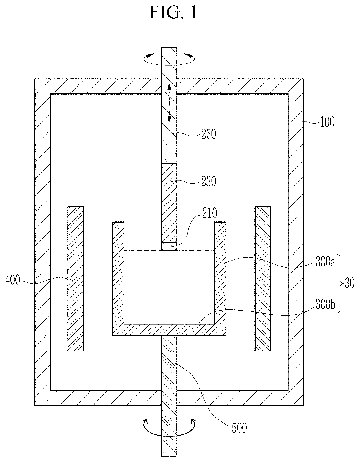
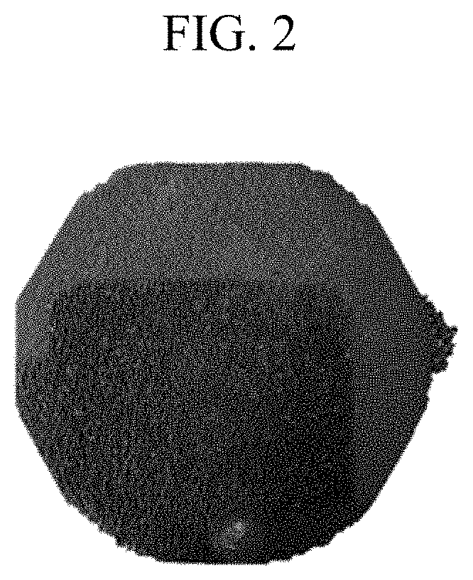
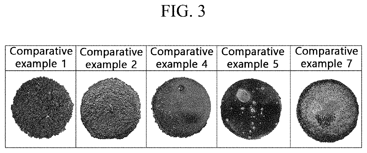
[0024]Exemplary embodiments of the present invention will be described in detail with reference to the accompanying drawings. In describing the present invention, a description of known functions or configurations will be omitted so as to make the subject matter of the present invention more clear.

[0025]To clearly describe the present invention, portions which do not relate to the description are omitted, and like reference numerals designate like elements throughout the specification. The size and thickness of each component shown in the drawings are arbitrarily shown for better understanding and ease of description, but the present invention is not limited thereto.

[0026]In the drawings, the thickness of layers, films, panels, regions, etc., are exaggerated for clarity. For better understanding and ease of description, the thicknesses of some layers and areas are exaggerated. It will be understood that when an element such as a layer, film, region, or substrate is referred to as be...


PUM


Abstract

A silicon-based molten composition according to an exemplary embodiment is used in a solution growing method for forming a silicon carbide single crystal, includes silicon (Si), yttrium (Y), and iron (Fe), and is expressed in Formula 1.SiaYbFec   [Formula 1]In Formula 1, the a is equal to or greater than 0.4 and equal to or less than 0.8,the b is equal to or greater than 0.2 and equal to or less than 0.3, and the c is equal to or greater than 0.1 and equal to or less than 0.2.

Description

CROSS-REFERENCE TO RELATED APPLICATION[0001]This application claims priority to and the benefit of Korean Patent Application No. 10-2018-0059815 filed in the Korean Intellectual Property Office on May 25, 2018, the entire contents of which are incorporated herein by reference.BACKGROUND OF THE INVENTION(a) Field of the Invention[0002]The present invention relates a silicon-based molten composition and a method for manufacturing silicon carbide single crystal using the same.(b) Description of the Related Art[0003]An electrical power semiconductor device is a key device for a next-generation system using electrical energy, such as an electric vehicle and an electric power system, or for radio frequency mobile communication. For this purpose, it is required to select a material that is appropriate for high voltage, high current, and radio frequency. Silicon single crystal has been used as an electrical power semiconductor material, but because of a limit of the physical property, silic...

Claims


Application Information

Patent Timeline
IPC IPC(8): C30B29/36C30B15/14
CPCC30B29/36C30B15/14C30B19/04C30B19/062C30B15/36
Inventor LEE, HORIMKIM, JUNGHWANCHUNG, CHANYEUPKO, JUNG MIN
Owner LG CHEM LTD
Why Eureka
Try Eureka