Semiconductor Chip, Method of Producing a Semiconductor Chip and Apparatus Having a Plurality of Semiconductor Chips

a semiconductor chip and semiconductor technology, applied in the direction of semiconductor devices, semiconductor/solid-state device details, electrical devices, etc., can solve the problems of reducing the breakage stability of the chips, reducing and reducing the breakage strength of the chips. , to achieve the effect of improving the breakage strength of the semiconductor chips, and reducing the number of semiconductor chips

Active Publication Date: 2020-05-28
OSRAM OLED
View PDF0 Cites 0 Cited by
  • Summary
  • Abstract
  • Description
  • Claims
  • Application Information

AI Technical Summary

Benefits of technology

The patent describes a method for making semiconductor chips by using a contact metallization on the bottom side of the substrate. This contact metallization can be made of various metals and alloys, and can be designed to mount and electrically contact the semiconductor chip. The contact metallization is applied to the substrate and is retracted in the lateral direction, so that it does not protrude beyond the bottom side of the substrate. This design prevents unwanted electrical connections between adjacent semiconductor chips and increases the breaking strength of the semiconductor chips. The method also allows for a separation of the substrate wafer and semiconductor chip using an etching process, resulting in a wider substrate and reduced solder bulgings. The method also includes a two-stage etching process that produces a wider substrate and reduces damage to the chip edge. Additionally, a fluoropolymer passivation can be applied to the chip side surfaces for protection and increased adhesion.

Problems solved by technology

However, this requires relatively wide mesa trenches between adjacent semiconductor chips.
The laser separation also causes mechanical damage at the chip edges and in the resulting melt.
This reduces the breakage stability of the chips.
In addition, the metallic contact layers terminate flush with the chip edges, so that there is a risk of short-circuiting these in a close assembly of two or more semiconductor chips.

Method used


Image

  • Semiconductor Chip, Method of Producing a Semiconductor Chip and Apparatus Having a Plurality of Semiconductor Chips
  • Semiconductor Chip, Method of Producing a Semiconductor Chip and Apparatus Having a Plurality of Semiconductor Chips
  • Semiconductor Chip, Method of Producing a Semiconductor Chip and Apparatus Having a Plurality of Semiconductor Chips

Examples


Embodiment Construction

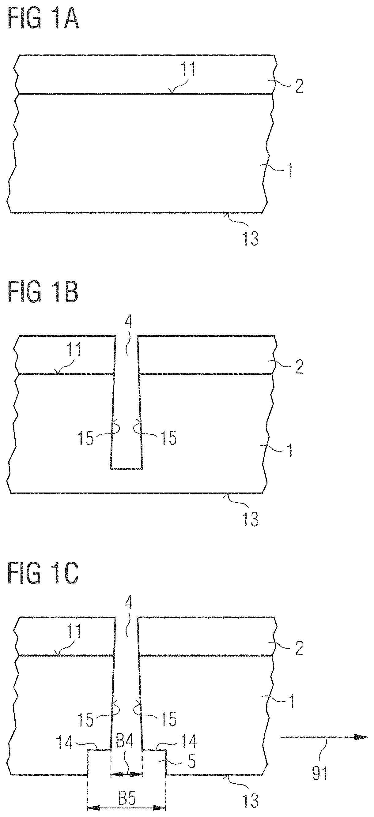
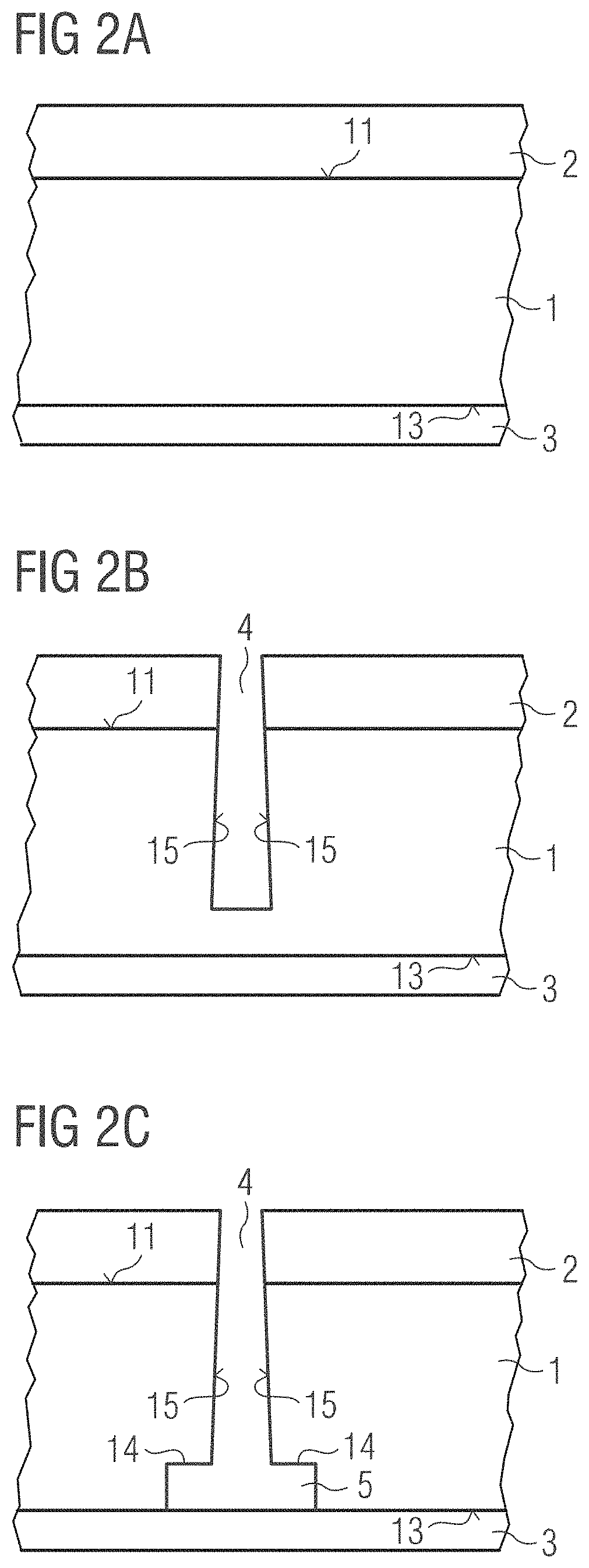
[0036]In connection with FIGS. 1A to 1F, a method for producing a semiconductor chip 100 and features of the semiconductor chip 100 are described. For this purpose, in a first method step, as shown in FIG. 1A, a substrate wafer 1, shown in a partial view, is provided with a semiconductor layer 2 applied thereon in large-area fashion. In particular, the substrate wafer 1 has a top side 11 facing the semiconductor layer and a bottom side 13 facing away from the semiconductor layer 2. The semiconductor layer 2, which can also be embodied as a semiconductor layer sequence with a plurality of semiconductor layers according to the description in the general part, can be grown on the top side 11 of the substrate wafer. Alternatively, it may also be possible that the semiconductor layer 2 has been grown on a growth substrate wafer and afterwards has been transferred onto the substrate wafer 1 formed by a carrier substrate wafer. Accordingly, the substrate wafer 1 may be either a growth subs...


PUM

PropertyMeasurementUnit
thicknessaaaaaaaaaa
thicknessaaaaaaaaaa
widthaaaaaaaaaa

Abstract

A semiconductor chip, a method for producing a semiconductor chip and an apparatus having a plurality of semiconductor chips are disclosed. In an embodiment a chip includes a substrate and a semiconductor layer arranged at the substrate, wherein the substrate includes, at a side facing the semiconductor layer, a top side with a width B1 in a first lateral direction and, at a side opposite to the top side, a bottom side with a width B3 in the first lateral direction, wherein the substrate has a width B2 in the first lateral direction at a half height between the top side and the bottom side, and wherein the following applies to widths B1, B2 and B3: B1-B2<B2-B3, and B1≥B2>B3.

Description

[0001]This patent application is a national phase filing under section 371 of PCT / EP2017 / 065286, filed Jun. 21, 2017, which claims the priority of German patent application 10 2016 112 584.9, filed Jul. 8, 2016, each of which is incorporated herein by reference in its entirety.TECHNICAL FIELD[0002]The present invention relates to a semiconductor chip, a method for producing a semiconductor chip and an apparatus with a plurality of semiconductor chips.BACKGROUND[0003]For the production of semiconductor chips usually a wafer is produced with a variety of desired semiconductor structures, said wafer then being singulated by means of splitting it up into a plurality of individual semiconductor chips. For this typically a laser separation process is used, in which a laser severs all layers including already applied metallic contact layers. However, this requires relatively wide mesa trenches between adjacent semiconductor chips. The laser separation also causes mechanical damage at the c...

Claims


Application Information

Patent Timeline
Patent Type & Authority Applications(United States)
IPC IPC(8): H01L21/78H01L21/28H01L23/538
CPCH01L23/538H01L21/78H01L21/28H01L33/20H01L2933/0033H01L25/0753
Inventor OTTO, ISABELRODE, PATRICK
Owner OSRAM OLED
Why Eureka
Try Eureka