
Semiconductor device

a semiconductor device and semiconductor technology, applied in semiconductor devices, instruments, transmission systems, etc., can solve the problems of reducing optical power, difficult to manufacture laser diodes, and difficult to align light modulators with laser diodes by narrow beams, so as to improve optical power of semiconductor devices, reduce the width of light emitted from light-emitting diodes, and improve the alignment between light-emitting parts and light-emitting parts

Active Publication Date: 2020-05-07
SUZHOU LEKIN SEMICON CO LTD
View PDF0 Cites 0 Cited by
  • Summary
  • Abstract
  • Description
  • Claims
  • Application Information

AI Technical Summary

Benefits of technology

The patent improves the optical power of semiconductor devices, improves the alignment between different parts, reduces the peak width of light emitted, improves the transmission and reduces noise, and increases the extinction ratio of the device. It also prevents light leakage and improves the performance of the semiconductor device.

Problems solved by technology

However, the laser diode is difficult to manufacture, and it is difficult to align a light modulator with the laser diode by a narrow beam.
Therefore, there is a problem that optical power is decreased.

Method used


Image

  • Semiconductor device
  • Semiconductor device
  • Semiconductor device

Examples


Embodiment Construction

lass="d_n">[0106]Embodiments of the present invention may be modified into other forms, or several embodiments may be combined with each other, and the scope of the present invention is not limited to each of the embodiments described below.

[0107]Although an item described in a specific embodiment is not described in other embodiment, unless otherwise described in the other embodiment or as long as there is no contradictory description therein, the item may be understood as being related to the other embodiment.

[0108]For example, when a feature for a configuration A is described in a specific embodiment and a feature for a configuration B is described in other embodiment, even when an embodiment in which the configuration A and the configuration B are combined is not explicitly described, unless otherwise described in the other embodiment or as long as there is no contradictory explanation therein, it should be understood that the combined embodiment will fall within the scope of th...


PUM

PropertyMeasurementUnit
conductiveaaaaaaaaaa
wavelengthsaaaaaaaaaa
thicknessaaaaaaaaaa

Abstract

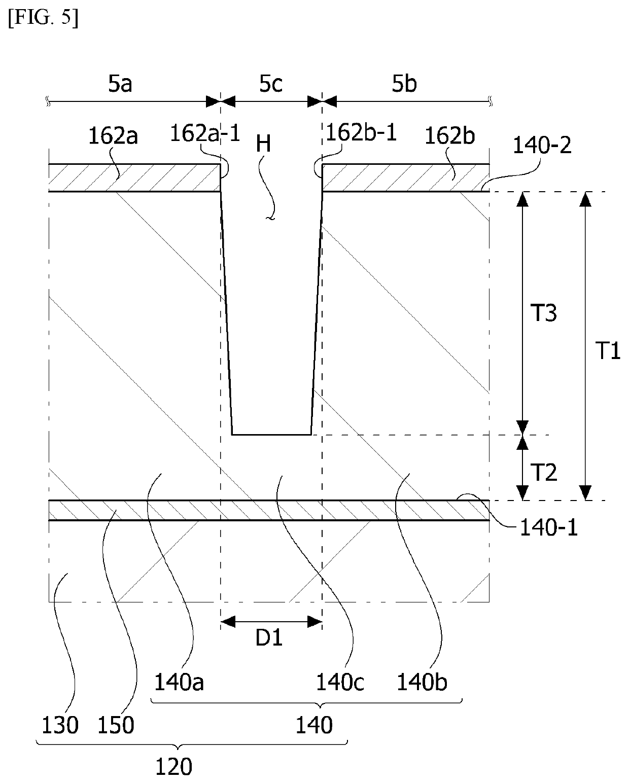
An embodiment discloses a semiconductor device comprising: a semiconductor structure comprising a first conductive semiconductor layer, a second conductive semiconductor layer, and an active layer disposed between the first conductive semiconductor layer and the second conductive semiconductor layer; a first electrode disposed on the first conductive semiconductor layer; a 2-1 electrode disposed on the second conductive semiconductor layer; and a 2-2 electrode disposed on the second conductive semiconductor layer and spaced apart from the 2-1 electrode, wherein the thickness of a part of the second conductive semiconductor layer between the 2-1 electrode and the 2-2 electrode is smaller than the thickness of the second conductive semiconductor layer vertically overlapping with the 2-1 electrode and the 2-2 electrode; the 2-2 electrode is opposite to the 2-1 electrode and comprises a first region that is closest to the 2-1 electrode; the 2-1 electrode is opposite to the 2-2 electrode and comprises a second region that is closest to the 2-2 electrode; and the relationship between the width (W1) of the first region and the width (W2) of the second region is W1≥W2.

Description

TECHNICAL FIELD[0001]Embodiments relate to a semiconductor device.BACKGROUND ART[0002]A semiconductor device including a compound, such as GaN and AlGaN, has many advantages, such as wide and adjustable band-gap energy, and thus may be diversely used for light-emitting devices, light-receiving devices, various diodes, and the like.[0003]In particular, a light-emitting device, such as a light-emitting diode or a laser diode, using a III-V group or II-VI group compound semiconductor material can realize various colors, such as red, green, and blue, or emit ultraviolet light, due to the development of thin-film growth technology and device materials. The light-emitting device can also emit efficient white light by using a fluorescent material or combining colors and has the advantages of low power consumption, semi-permanent lifetime, high response speed, safety, and environmental friendliness as compared to existing light sources such as fluorescent lamps and incandescent lamps.[0004]...

Claims


Application Information

Patent Timeline
Patent Type & Authority Applications(United States)
IPC IPC(8): H01L33/58H01L33/38H01L33/46H01L33/32H01L33/10
CPCH01L33/10H01L33/387H01L33/58H01L33/32H01L33/46G08C23/04H01L27/15H01L33/06H01L33/20
Inventor KIM, SEUNG HWANKIM, WON HOKIM, CHONG COOKSEO, DEOK WONYOON, YEO JAECHOI, KWANG KI
Owner SUZHOU LEKIN SEMICON CO LTD
Learn More