Manufacturing apparatus for performing additive manufacturing of an electrical device

a manufacturing apparatus and additive manufacturing technology, applied in the direction of printed circuit manufacturing, manufacturing tools, conductive pattern formation, etc., can solve the problems of lack of smooth work process transition, and achieve the effect of quick shaping of multi-layer wiring boards, reducing the length of the movement time of the stage, and enhancing versatility

Active Publication Date: 2020-03-19
FUJI CORP
View PDF3 Cites 2 Cited by
  • Summary
  • Abstract
  • Description
  • Claims
  • Application Information

AI Technical Summary

Benefits of technology

[0006]The present disclosure has been made in view of the above-described circumstances, and an object thereof is to provide a manufacturing apparatus and a manufacturing method allowing the length of time required for a work process transition to be reduced in a manufacturing apparatus that manufactures an electrical device using additive manufacturing.
[0022]In the manufacturing apparatus according to claim 7 of the present application, the arrangement of the shaping unit and the mounting unit is determined such that the path length of the stage moved as a result of the progress of the work process is minimized. Accordingly, a user of the manufacturing apparatus or the like can reduce the length of the movement time of the stage moving between the units during the work process transition by, for example, changing the direction of each of the units with respect to the movement direction of the stage in accordance with an instruction given by the manufacturing apparatus or the like.

Problems solved by technology

As a result, the three-dimensional article needs to be rearranged and repositioned during a movement between the devices, which results in the lack of a smooth work process transition.

Method used


Image

  • Manufacturing apparatus for performing additive manufacturing of an electrical device
  • Manufacturing apparatus for performing additive manufacturing of an electrical device
  • Manufacturing apparatus for performing additive manufacturing of an electrical device

Examples


Embodiment Construction

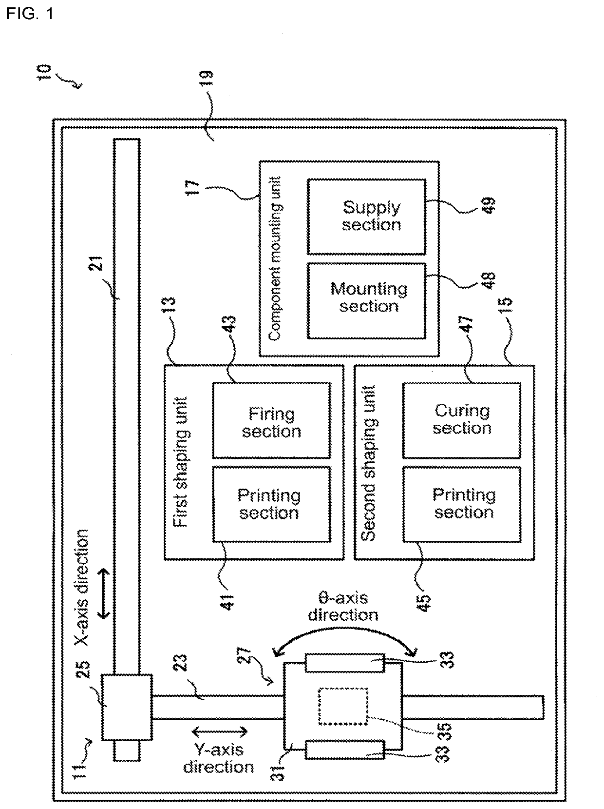
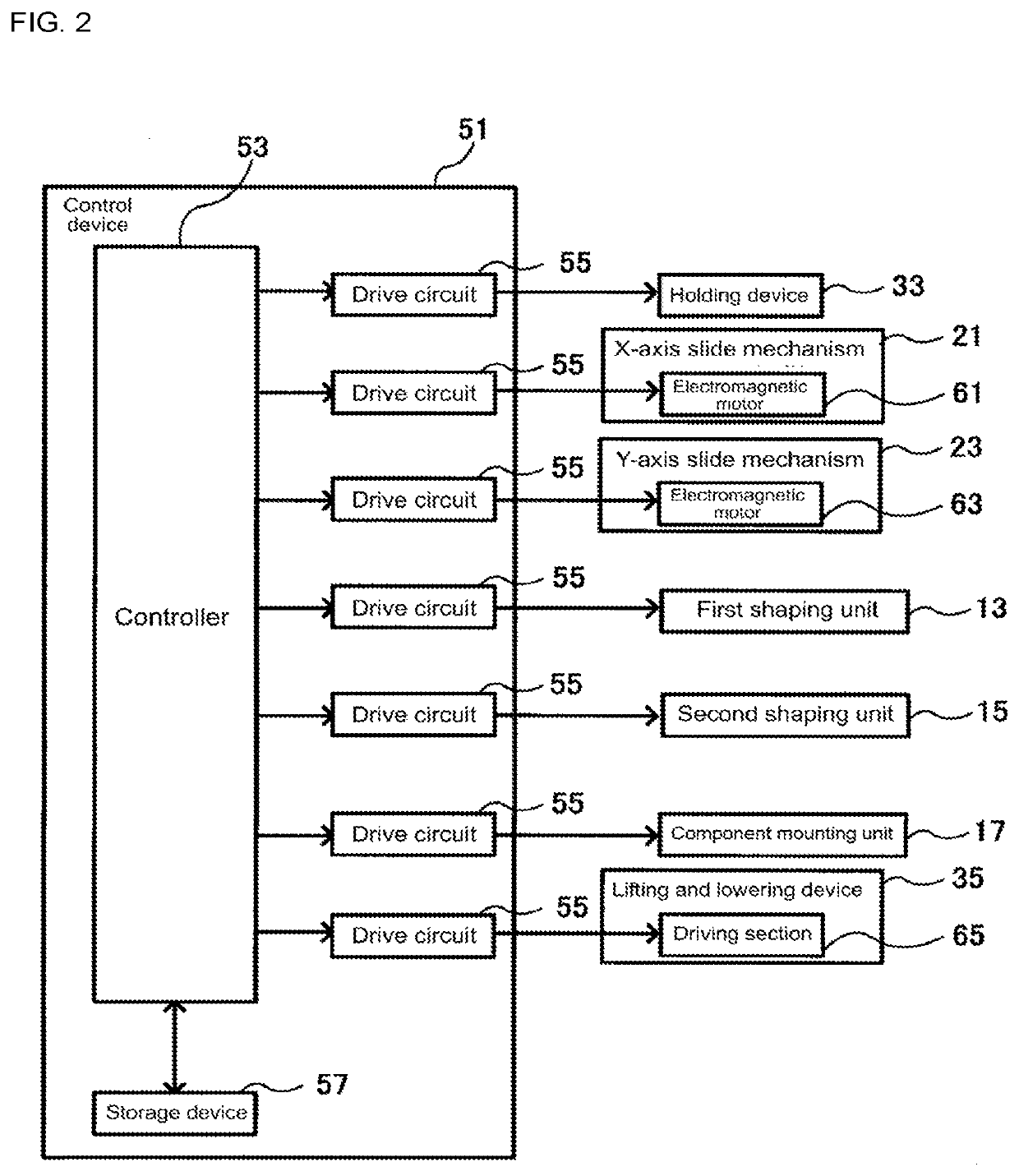
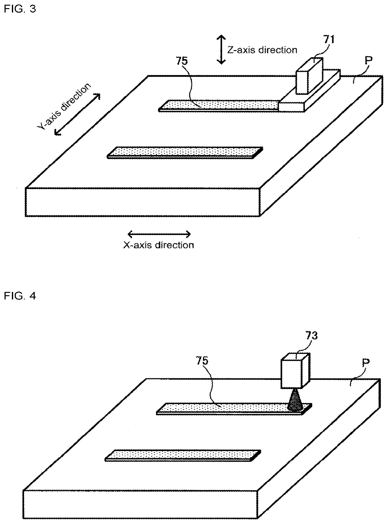
[0037]Hereinafter, an electronic device manufacturing apparatus as an embodiment of a manufacturing apparatus according to the present disclosure will be described with reference to the accompanying drawings. FIG. 1 is a diagram illustrating a configuration of electronic device manufacturing apparatus (hereinafter, simply referred to as a “manufacturing apparatus” in some cases) 10 according to the present embodiment. Manufacturing apparatus 10 is provided with conveyance device 11, first shaping unit 13, second shaping unit 15, and component mounting unit 17. In manufacturing apparatus 10, units 13, 15, and 17 and so on are arranged on base 19. Base 19 has a substantially rectangular shape in a plan view. In the following description, a longitudinal direction of base 19 will be referred to as an X-axis direction, a short direction of base 19 will be referred to as a Y-axis direction, a direction that is orthogonal to both the X-axis direction and the Y-axis direction will be referr...


PUM

PropertyMeasurementUnit
conductiveaaaaaaaaaa
lengthaaaaaaaaaa
thicknessaaaaaaaaaa

Abstract

A manufacturing apparatus that includes a conveyance device that moves a stage, where an electronic device shaped by multiple layers is placed, in X-axis and Y-axis directions. A first shaping unit, a second shaping unit, and a component mounting unit are arranged within a range in which the stage can move. The manufacturing apparatus performs additive manufacturing of the electronic device on the stage by performing a sequential movement of the stage to respective working positions of different units. As a result, in this manufacturing apparatus, a workpiece on the stage does not have to be removed and repositioned during each work process such as shaping by a first shaping unit, shaping by a second shaping unit, and electronic component mounting by a component mounting unit.

Description

CROSS-REFERENCE TO RELATED APPLICATIONS[0001]This application is a division of U.S. application Ser. No. 15 / 512,101, filed Mar. 17, 2017, which is a National Stage of International Application No. PCT / JP2014 / 074829, filed Sep. 19, 2014, the entire contents of which are incorporated herein by reference.TECHNICAL FIELD[0002]The present application relates to a manufacturing apparatus and a manufacturing method for manufacturing an electrical device by using additive manufacturing.BACKGROUND ART[0003]An example of a three-dimensional article manufacturing method is additive manufacturing, in which a three-dimensional article is manufactured by sequentially stacking layers of materials for forming a three-dimensional article to be formed of multiple layers. Stereo lithography (SL), selective laser sintering (SLS), fused deposition molding (FDM), and the like are known as forms of additive manufacturing. For example, in the manufacturing apparatus that is disclosed in PTL 1, a flat plate...

Claims


Application Information

Patent Timeline
Patent Type & Authority Applications(United States)
IPC IPC(8): H05K3/00H05K3/10B29C67/00B23P21/00B33Y10/00B33Y30/00B33Y80/00H05K3/46H05K1/09H05K3/12B22F3/105
CPCH05K3/4664H05K2203/107H05K3/1241H05K3/103H05K2203/1131B33Y30/00B22F3/105B23P21/004H05K3/0008B33Y10/00B29C67/0003H05K1/097B29C67/00B33Y80/00H05K3/0014
Inventor SUZUKI, MASATOKAWAJIRI, AKIHIROFUJITA, MASATOSHITSUKADA, KENJIHASHIMOTO, YOSHITAKA
Owner FUJI CORP
Why Eureka
Try Eureka