Semiconductor device
a technology of semiconductor devices and semiconductors, applied in semiconductor devices, diodes, electrical equipment, etc., can solve the problems of increasing recovery current and withstand voltage drop, and achieve the effects of reducing the amount of holes supplied, increasing manufacturing steps, and inhibiting an increase in recovery curren
- Summary
- Abstract
- Description
- Claims
- Application Information
AI Technical Summary
Benefits of technology
Problems solved by technology
Method used
Image

Examples
first embodiment
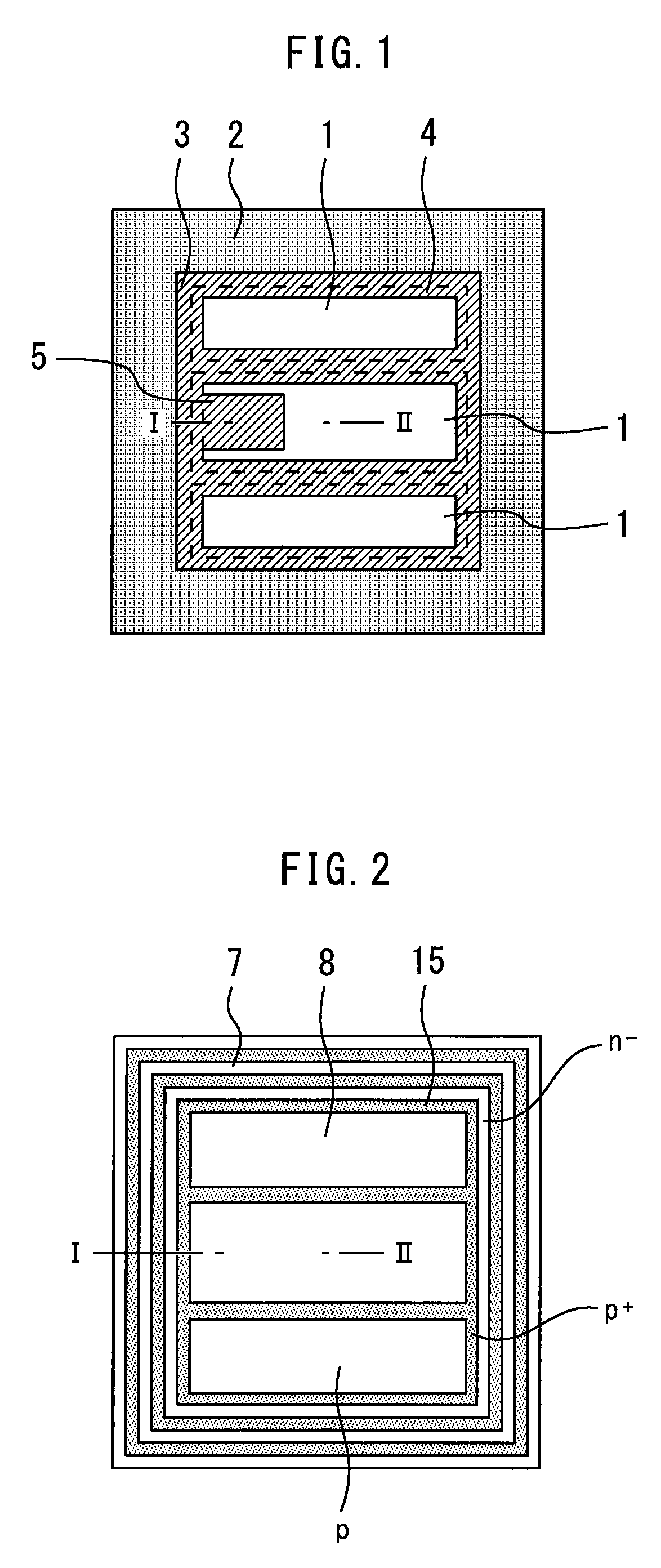
[0022]FIG. 1 is a top view illustrating a region of a semiconductor device according to a first embodiment. A termination region 2 for retaining a withstand voltage is located around a cell region 1 of an RC-IGBT. A wiring region 3 is positioned between the cell region 1 and the termination region 2 or between the cell regions 1. A gate wiring 4 and a gate pad 5 are provided in this wiring region 3. The region including the cell region 1 enclosed by the wiring region 3 is called an “active region” to distinguish it from the termination region 2.
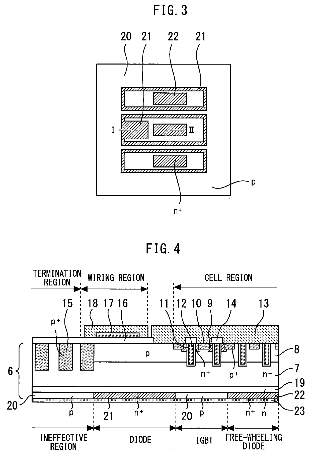
[0023]FIG. 2 is a top view illustrating the semiconductor substrate according to the first embodiment. FIG. 3 is a bottom view illustrating the semiconductor substrate according to the first embodiment. FIG. 4 is a cross-sectional view illustrating the semiconductor device according to the first embodiment and corresponds to cross-sectional views along I-II in FIGS. 1 to 3. An IGBT and a free-wheeling diode are provided in the cell region.
[00...
second embodiment
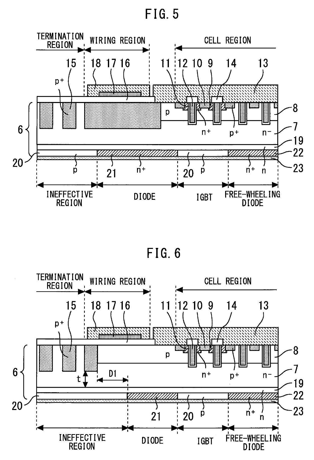
[0032]FIG. 6 is a cross-sectional view illustrating a semiconductor device according to a second embodiment. In the present embodiment, a distance D1 from the p+-type well layer 15 having a high impurity concentration and a large depth to the n+-type cathode layer 21 is set to be equal to or greater than a thickness t of the n−-type drift layer 7 right below the p+-type well layer 15. Thus, making the distance D1 from the p+-type well layer 15 to the n+-type cathode layer 21 wider can inhibit the supply of holes from the n+-type cathode layer 21 and reduce recovery current. When an angle at which holes spread from the p+-type well layer 15 on the surface side toward the n+-type cathode layer 21 on the reverse side is assumed to be 45°, the distance D1 should be equal to or greater than the thickness t of the n−-type drift layer 7 to inhibit the supply of holes from the n+-type cathode layer 21.
third embodiment
[0033]FIG. 7 is a cross-sectional view illustrating a semiconductor device according to a third embodiment. According to the present embodiment, a p+-type emitter layer 24 having a higher impurity concentration than the p-type base layer 8 is provided on the surface side of the p-type base layer 8 in the wiring region. This makes it possible to reduce resistance of contact with the surface electrode 13 and reduce forward direction loss. When a barrier metal such as Ti, TiN or TiW is formed on the surface electrode 13 in particular, good ohmic contact with the barrier metal can be obtained by increasing impurity concentration on a joint surface.
[0034]Furthermore, the p+-type emitter layer 24 is away from the p+-type well layer 15 by a distance D2 and the p-type base layer 8 having a relatively low impurity concentration is provided between both layers to prevent their connection. It is thereby possible to inhibit the supply of holes from the p+-type well layer 15 and inhibit an incre...
PUM
 Abstract
Description
Claims
Application Information
 - R&D
- Intellectual Property
- Life Sciences
- Materials
- Tech Scout
- Unparalleled Data Quality
- Higher Quality Content
- 60% Fewer Hallucinations
Browse by: Latest US Patents, China's latest patents, Technical Efficacy Thesaurus, Application Domain, Technology Topic, Popular Technical Reports.
© 2025 PatSnap. All rights reserved.Legal|Privacy policy|Modern Slavery Act Transparency Statement|Sitemap|About US| Contact US: help@patsnap.com