
Electronic component and electronic component device

Active Publication Date: 2019-03-14
TDK CORPARATION
View PDF7 Cites 5 Cited by
  • Summary
  • Abstract
  • Description
  • Claims
  • Application Information

AI Technical Summary

Benefits of technology

The present invention aims to provide an electronic component with a conductive resin layer that is less likely to peel off from the main element and has better resistance to moisture damage. The invention also provides an electronic component device that includes a conductive resin layer that is less likely to peel off and has improved moisture resistance reliability.

Problems solved by technology

In a case where moisture infiltrates from the region between the element body and the conductive resin layer, durability of the electronic component decreases.

Method used


Image

  • Electronic component and electronic component device
  • Electronic component and electronic component device
  • Electronic component and electronic component device

Examples


first embodiment

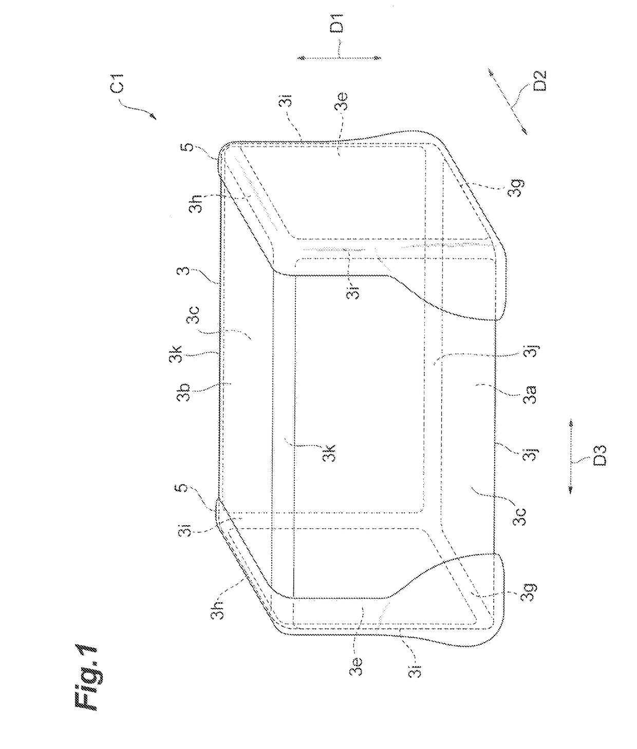
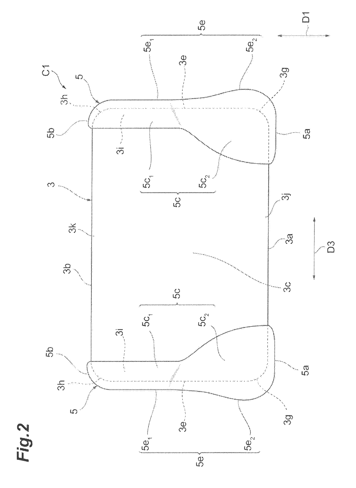
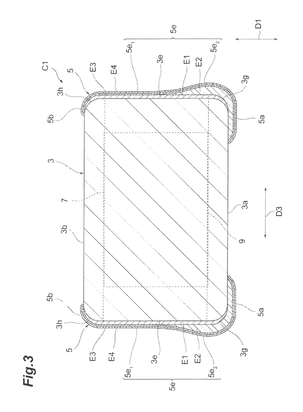
[0037]A configuration of a multilayer capacitor C1 according to a first embodiment will be described with reference to FIGS. 1 to 8. FIG. 1 is a perspective view of the multilayer capacitor according to the first embodiment. FIG. 2 is a side view of the multilayer capacitor according to the first embodiment. FIGS. 3 to 5 are views illustrating a cross-sectional configuration of the multilayer capacitor according to the first embodiment. FIG. 6 is a plan view illustrating an element body, a first electrode layer, and a second electrode layer. FIG. 7 is a side view illustrating the element body, the first electrode layer, and the second electrode layer. FIG. 8 is an end view illustrating the element body, the first electrode layer, and the second electrode layer. In the first embodiment, an electronic component is, for example, the multilayer capacitor C1.

[0038]As illustrated in FIG. 1, the multilayer capacitor C1 includes an element body 3 of a rectangular parallelepiped shape and a ...

second embodiment

[0101]With reference to FIGS. 10 to 17, a configuration of a multilayer feedthrough capacitor C3 according to a second embodiment will be described. FIGS. 10 and 11 are plan views of the multilayer feedthrough capacitor according to the second embodiment. FIG. 12 is a side view of the multilayer feedthrough capacitor according to the second embodiment. FIG. 13 is an end view of the multilayer feedthrough capacitor according to the second embodiment. FIGS. 14, 15, and 16 are views illustrating a cross-sectional configuration of the multilayer feedthrough capacitor according to the second embodiment. FIG. 17 is a side view illustrating an element body, a first electrode layer, and a second electrode layer. In the second embodiment, an electronic component is, for example, the multilayer feedthrough capacitor C3. Hereinafter, differences between the multilayer capacitor C1 and the multilayer feedthrough capacitor C3 will be mainly described.

[0102]As illustrated in FIGS. 10 to 13, the m...


PUM

PropertyMeasurementUnit
Electrical conductoraaaaaaaaaa
Heightaaaaaaaaaa

Abstract

An element body of a rectangular parallelepiped shape includes a first principal surface arranged to constitute a mounting surface, a second principal surface opposing the first principal surface in a first direction, a pair of side surfaces opposing each other in a second direction, and a pair of end surfaces opposing each other in a third direction. An external electrode is disposed at an end portion of the element body in the third direction. The external electrode includes a conductive resin layer. The conductive resin layer covers a region near the first principal surface of the end surface. A height of the conductive resin layer in the first direction is larger at an end portion in the second direction than at a center in the second direction, when viewed from the third direction.

Description

BACKGROUND OF THE INVENTION1. Field of the Invention[0001]The present invention relates to an electric component and an electric component device.2. Description of Related Art[0002]Known electronic components include an element body of a rectangular parallelepiped shape and a plurality of external electrodes (see, for example, Japanese Unexamined Patent Publication No. H8-107038). The element body includes a pair of principal surfaces opposing each other, a pair of end surfaces opposing each other, and a pair of side surfaces opposing each other. The plurality of external electrodes is disposed at each end portion of the element body in a direction in which the pair of end surfaces opposes each other. The external electrode includes a conductive resin layer covering the entire end surface.SUMMARY OF THE INVENTION[0003]An object of one aspect of the present invention is to provide an electronic component including a conductive resin layer that tends not to peel off from an element bo...

Claims


Application Information

Patent Timeline
IPC IPC(8): H01G4/248H01G4/232H05K1/11H05K1/18H01G4/30H05K1/02
CPCH01G4/248H01G4/2325H05K1/111H05K1/181H01G4/30H05K1/0271H05K2201/10015H01G4/1227H01G4/1236H01G4/1245H01G4/012H01G4/232H05K3/3442H05K2201/10636Y02P70/50
Inventor ONODERA, SHINYATAMURA, TAKEHISATAKEDA, ATSUSHIMORITA, KEN
Owner TDK CORPARATION
Learn More