
Electrooptic device based on multiple domain scattering effect

a scattering effect and optical device technology, applied in the field of optical device based on multiple domain scattering effect, can solve the problems of insufficient broadband to cover the entire visible spectral range, inability to use multiplex driving, and pdlcs can only be used as single pixel devices, etc., to achieve efficient light scattering and diffraction, low power consumption, and low cost

Active Publication Date: 2018-09-13
THE HONG KONG UNIV OF SCI & TECH
View PDF3 Cites 2 Cited by
  • Summary
  • Abstract
  • Description
  • Claims
  • Application Information

AI Technical Summary

Benefits of technology

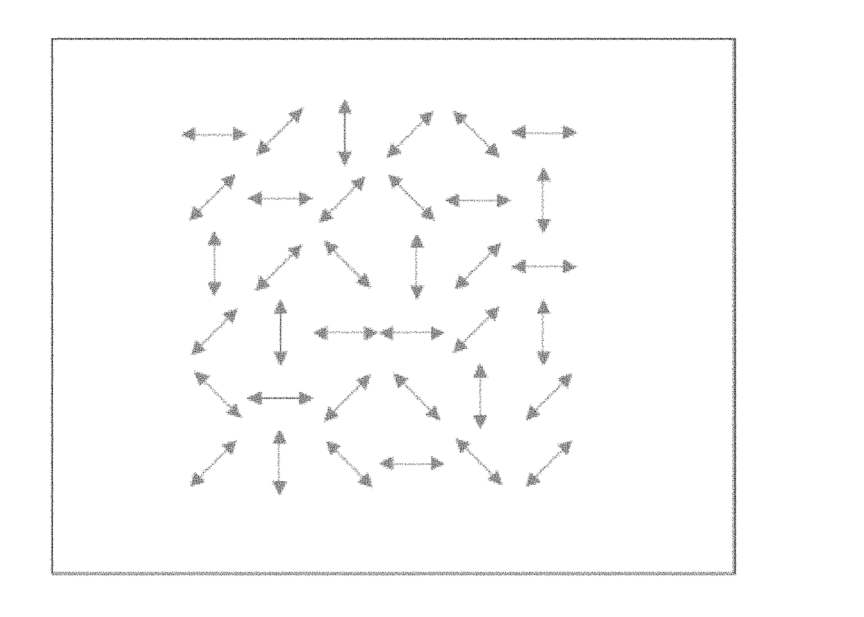
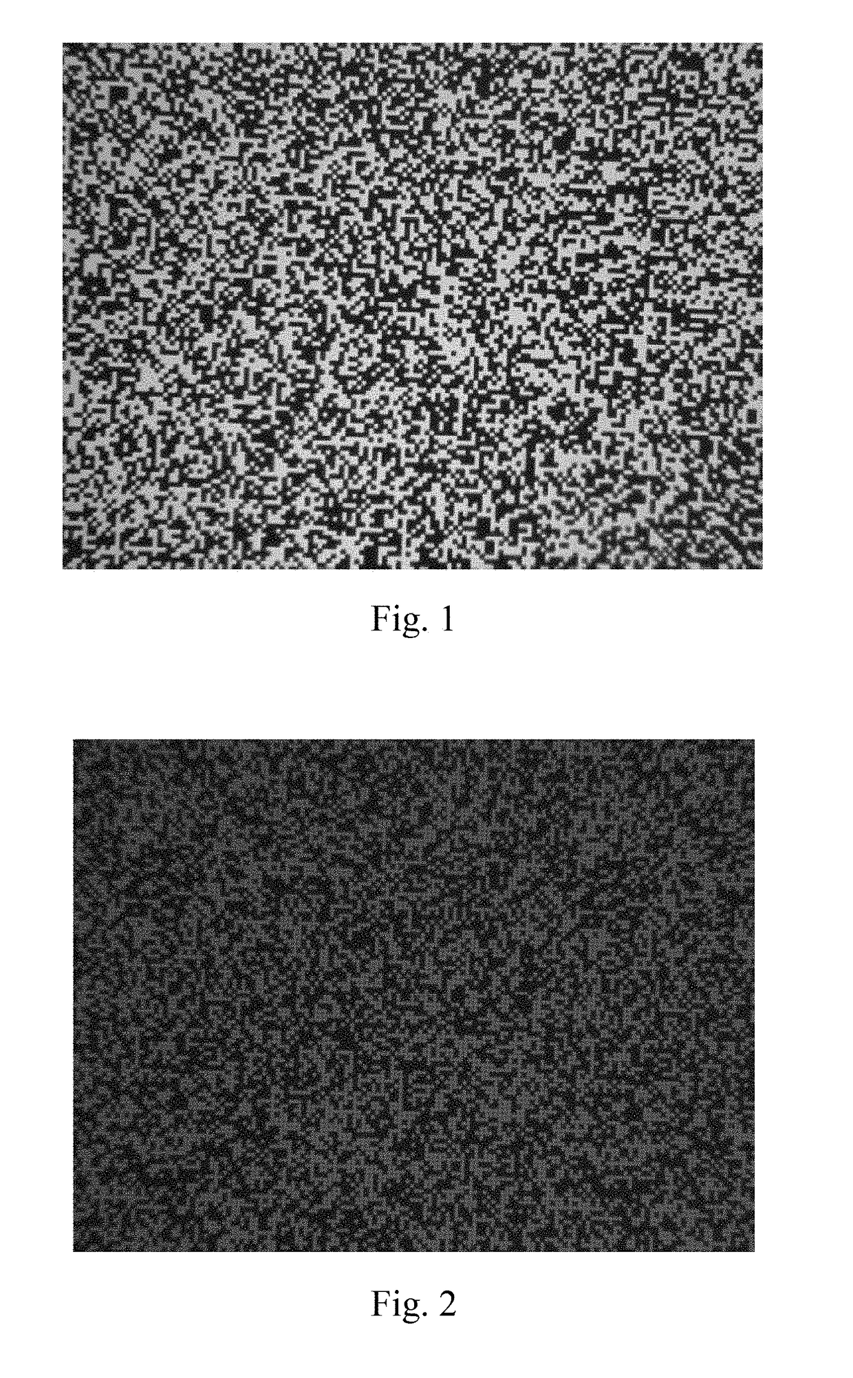
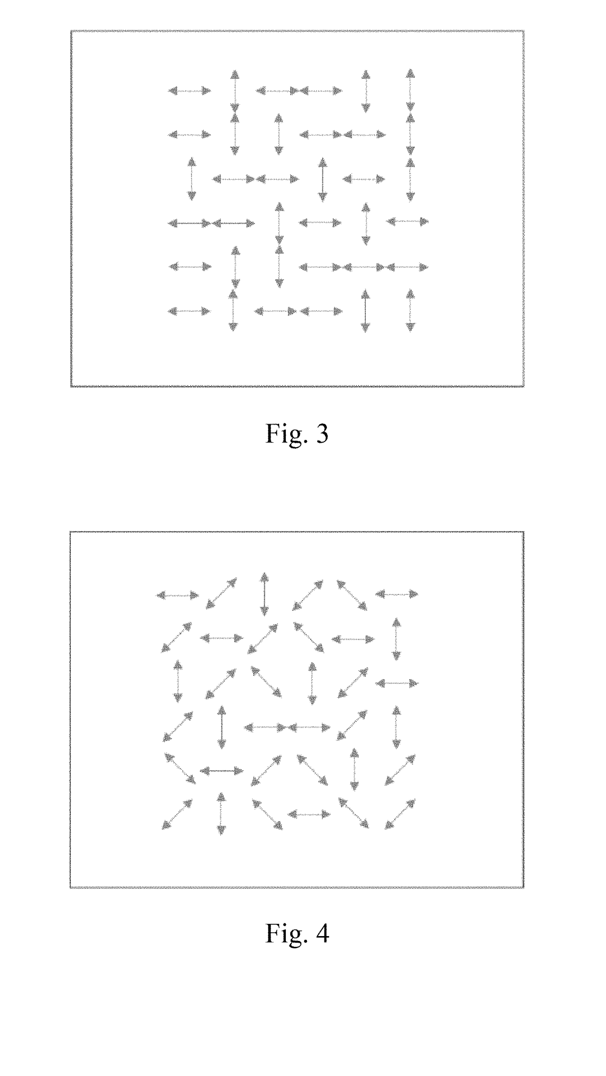
The invention provides an electronically tunable field-effect liquid crystal device that does not require polarizers and is bright, transmissive. It can be used for displays, light shutters, smart windows, and other applications. The device exhibits efficient light scattering and diffraction due to a uniquely designed and fabricated multi-domain liquid crystal configuration. The liquid crystal domains are patterned and each exhibits a designed orientation and geometry of its liquid crystal alignment. The orientation is not randomly generated, but in a dedicated random process chosen to result in optimal electro-optical performance. The alignment of the liquid crystal director within the domains can be planar or vertical, and the orientation of planar alignment and / or the pre-tilt direction can be controlled in more than one direction.

Problems solved by technology

The problem with ChLCD is that it does not provide enough broadband to cover the entire visible spectral range.
Moreover, since the size of the pockets or droplets of liquid crystal is random, the change between light-scattering and transmission is a very sluggish function of applied voltage, making multiplex driving impossible.
Thus, PDLCs can only be used as single pixel devices and are therefore not suitable for display applications.
These basic drawbacks prevent displaying adequate information contents and CMOS addressing of PDLCs.
Moreover, the large driving voltage and rather thick PDLC-layers required for adequate light scattering further limits the applicability of PDLCs.

Method used


Image

  • Electrooptic device based on multiple domain scattering effect
  • Electrooptic device based on multiple domain scattering effect
  • Electrooptic device based on multiple domain scattering effect

Examples


embodiment 1

[0044]A liquid crystal electro-optical field-effect device, the device comprising:

[0045]a liquid crystal cell comprising two substrates; and

[0046]at least one electrode electrically connected to at least one of the substrates,

[0047]wherein the electrode is transparent and / or patterned, and

[0048]wherein at least one substrate comprises a liquid crystal alignment layer having a multi-domain liquid crystal alignment.

embodiment 2

[0049]The device of embodiment 1, wherein the domains have at least one of a basically planar or a basically vertical LC-aligning direction.

embodiment 3

[0050]The device of embodiment 1, wherein each substrate is a liquid crystal alignment layer, and wherein one liquid alignment layer has a basically planar alignment and the other liquid crystal alignment layer has a basically vertical alignment.


PUM

PropertyMeasurementUnit
Lengthaaaaaaaaaa
Angleaaaaaaaaaa
Angleaaaaaaaaaa

Abstract

Devices and method of fabrication a liquid crystal electro-optic device which is based on light scattering and diffraction from a multiple domain field-effect liquid crystal configuration are provided. The multiple domains include random liquid crystal alignment directions fabricated by photo-alignment and have sizes ranging from sub-micrometer to several micrometers. The random alignment in the plane can be of two or more directions whereas the pretilt angle can vary between zero and 90°. The randomness of the planar directions of the liquid crystal director can be generated by a designed photo mask in combination with uniaxial photo-alignment.

Description

CROSS-REFERENCE TO RELATED APPLICATION[0001]This application claims the benefit of U.S. Provisional Application Ser. No. 62 / 600,858, filed Mar. 7, 2017, which is herein incorporated by reference in its entirety.FIELD OF INVENTION[0002]This invention deals with a field-effect mode of operation of a liquid crystal display and / or light shutter that is based on light scattering and diffraction by a multiple domain liquid crystal configuration.BACKGROUND[0003]Liquid crystal displays (LCDs) are dominant in the flat panel market. Almost all LCDs are based on nematic field effects. As such, LCDs acts as electro-optical polarization controllers. The nematic liquid crystal configurations in an LCD are aligned basically planar, vertically or twisted. The configurations serve to alter the polarization state of the incoming light. Light is transmitted or reflected between polarizers, depending on the polarization state of the output light from the liquid crystal configuration. Polarizers are ess...

Claims


Application Information

Patent Timeline
IPC IPC(8): G02F1/1337G02F1/1343
CPCG02F1/133711G02F1/133788G02F1/13439G02F2001/133738G02F2001/133742G02F1/133753G02F1/133738G02F1/133742G02F1/133761G02F1/133773
Inventor KWOK, HOI SINGSCHADT, MARTINFAN, FAN
Owner THE HONG KONG UNIV OF SCI & TECH
Learn More