
Mixed tin and germanium perovskites

a technology of germanium perovskites and mixed tin, which is applied in the direction of photovoltaic energy generation, electrical apparatus, semiconductor devices, etc., can solve the problems of reducing device efficiency, affecting the efficiency of devices, and affecting outdoor applications. , to achieve the effect of small effective mass, small positive value, and large positive valu

Inactive Publication Date: 2018-09-06
BROWN UNIVERSITY +1
View PDF2 Cites 8 Cited by
  • Summary
  • Abstract
  • Description
  • Claims
  • Application Information

AI Technical Summary

Benefits of technology

The patent text describes two new perovskite materials, which are compounds used in photovoltaic cells. The materials have different formulas and can be made in different ways. The technical effect of this patent is to provide new materials for improving the efficiency of photovoltaic cells. These materials can be used in cells made using different processes and can help to create more effective solar cells.

Problems solved by technology

However, there are obstacles yet to be overcome for outdoor applications.
Moreover, most lead-containing perovskites tend to degrade in the presence of moisture, a challenging issue for long-term outdoor usage.
For example, the photovoltaic devices based on the FAPbI3 have shown PCE up to 20%; but the FAPbI3 tends to transform from the black phase to yellow phase, resulting in dramatically reduced device efficiency.

Method used


Image

  • Mixed tin and germanium perovskites
  • Mixed tin and germanium perovskites
  • Mixed tin and germanium perovskites

Examples


example 1

[0037]CsSn0.5Ge0.5I3 perovskite material was synthesized by solid-state reaction in evacuated quartz tubes. Stoichiometric amounts of CsI, GeI2, SnI2 (available from Sigma Aldrich, USA) were placed in quartz tubes and evacuated to about 1×10⁻⁶ Torr and sealed using an oxy-methane torch. The evacuated tube was heated to 430° C. at 10° C. / min and held for 72 hours at 430° C. before slowly cooling the tube to room temperature at 10° C. / min. The sealed tube was opened in a glove box filled with nitrogen gas for further characterization / testing.

[0038]A thin film of CsSn0.5Ge0.5I3 perovskite material was prepared by flash evaporation as is known in the art of the as-synthesized CsSn0.5Ge0.5I3 powders directly.

example 2

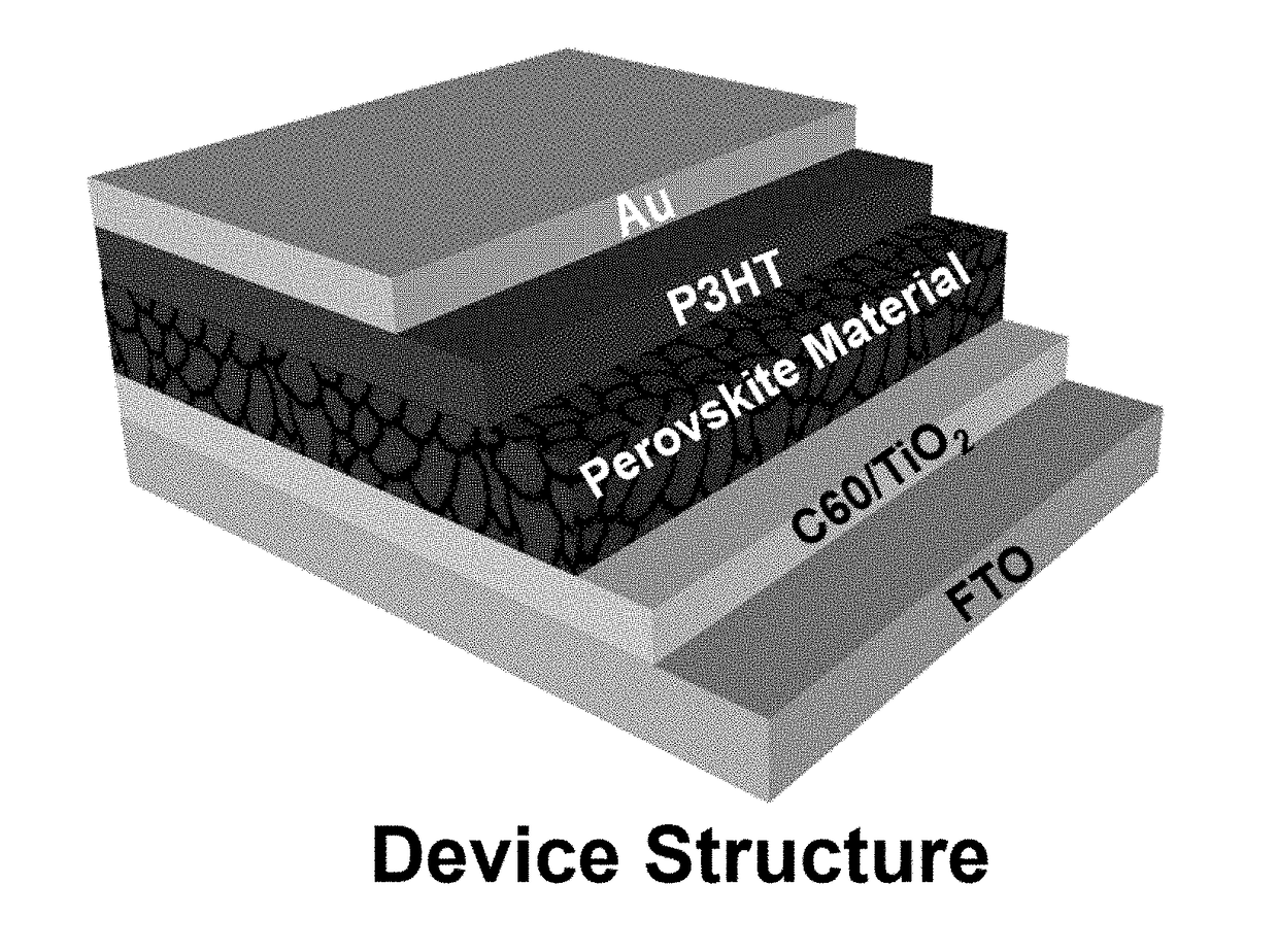
[0039]A photovoltaic cell was fabricated using the CsSn0.5Ge0.5I3 perovskite material synthesized in Example 1. Chemically etched FTO glass (available from Nippon Sheet Glass) was cleaned with detergent solution, acetone, and isopropanol. To form a 20 to 25 nm compact titanium dioxide (“TiO2”) electron-transporting layer, diluted titanium diisopropoxide bis(acetylacetonate) (“TAA”) solution (available from Sigma-Aldrich) in ethanol (0.2 ml of TAA in 6 ml of anhydrous ethanol) was sprayed at 450° C. A thin film of CsSn0.5Ge0.5I3 from Example 1 was then deposited. After evaporation, the prepared CsSn0.5Ge0.5I3 was cooled to room temperature in the vacuum chamber. A hole-transporting material (“HTM”) solution for forming an HTM layer was prepared by dissolving 10 mg of poly(3-hexylthiophene-2,5-diyl) (“P3HT”) in 1 mL of toluene. An HTM layer was formed on the thin film of CsSn0.5Ge0.5I3 by spin-coating the HTM solution at 3000 rpm for 15 s, and followed by the deposition of the 80 nm t...


PUM


Abstract

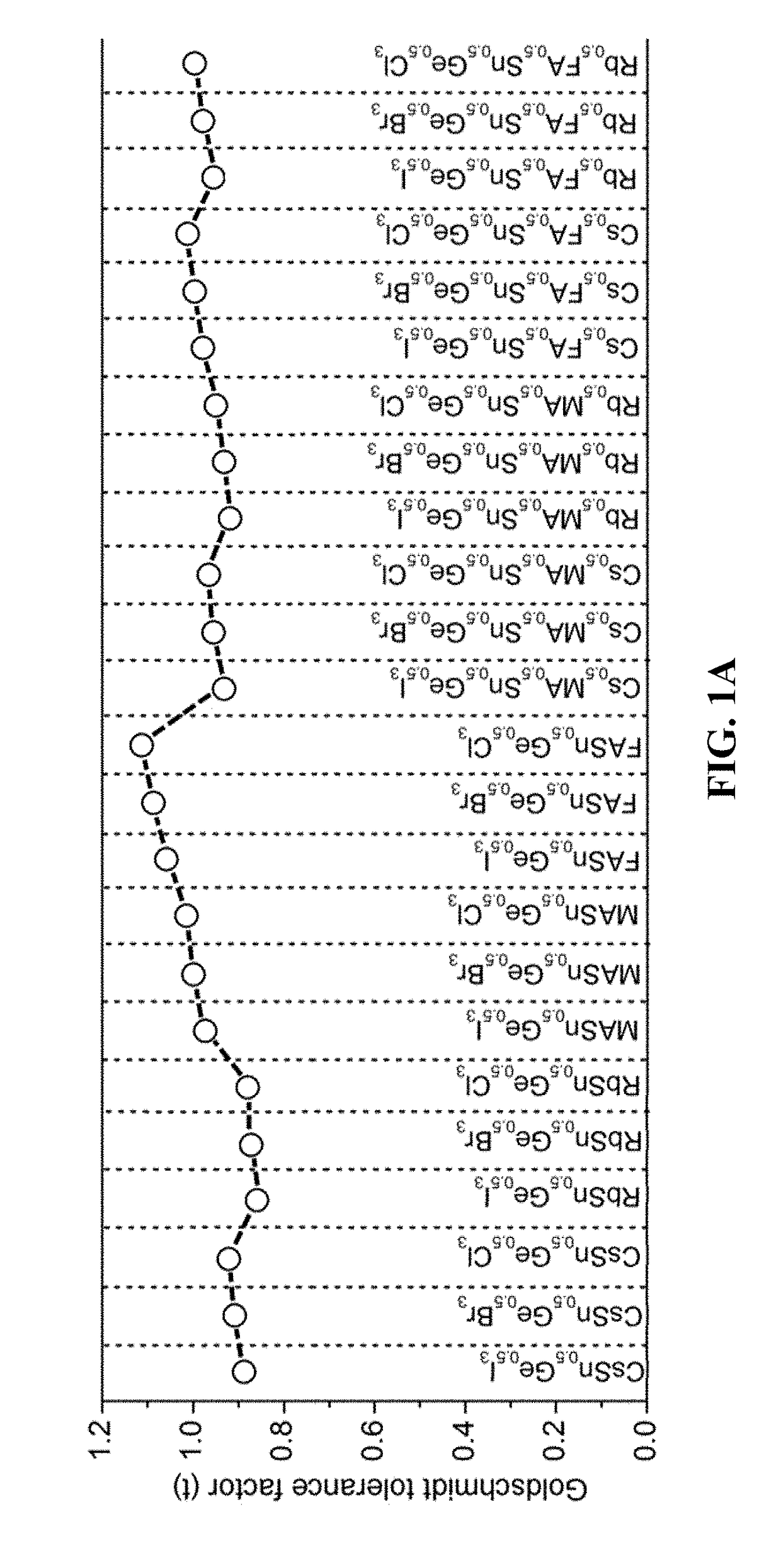
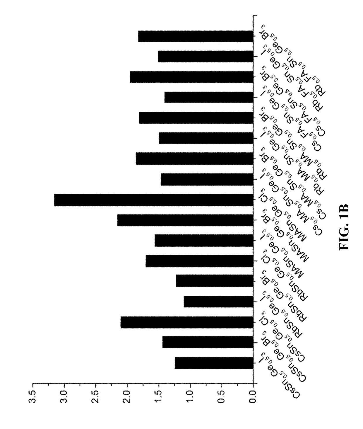
Perovskite materials useful in the manufacture of photovoltaic cells are provided. The perovskite materials have the formula AB′0.5B″0.5X3 or A′0.5A″0.5B′0.5B″0.5X3, wherein A, A′, and A″ are organic or inorganic cations, X is a halogen ion, B′ is tin, and B″ is germanium. Embodiments of the mixed tin and germanium halide perovskite materials possess a direct bandgap within the optimal range of 0.9-1.6 eV and have an optical absorption spectrum that is comparable to the state-of-the-art methylammonium lead iodide perovskites. The perovskite materials provided herein have been formulated to be lead-free.

Description

[0001]This application is a nonprovisional application claiming the benefit of U.S. Provisional Patent Application Ser. No. 62 / 465,559, filed Mar. 1, 2017, the disclosure of which is incorporated herein by reference in its entirety.STATEMENT REGARDING FEDERALLY SPONSORED RESEARCH OR DEVELOPMENT[0002]This invention was made with Government support under project numbers OIA-1538893 / 2611230129003 and DMR-1420645 by the National Science Foundation. The Government has certain rights in the invention.BACKGROUND[0003]Inorganic-organic halide perovskites represent a major break-through in the development of highly efficient photovoltaic materials. Within only several years, polycrystalline thin-film perovskite photovoltaic (“PV”) devices have achieved power conversion efficiency (“PCE”) of 22.1%. The rapid rise in PCE, coupled with the prospect of low-cost precursors and facile synthesis, render the perovskite photovoltaic devices highly competitive for commercial applications.[0004]However...

Claims


Application Information

Patent Timeline
IPC IPC(8): H01L31/032H01L51/42H01L31/04
CPCH01L31/032H01L51/4213H01L31/04C01P2002/34Y02E10/549H10K30/151H10K30/10H10K30/50H10K85/50
Inventor ZENG, XIAO CHENGJU, MINGGANGPADTURE, NITINZHOU, YUANYUANCHEN, MIN
Owner BROWN UNIVERSITY
Learn More