Electric-power converting device, solar power conditioner system, electricity storage system, uninterruptible power source system, wind power generation system, and motor drive system

a technology of electric-power conversion and conversion device, which is applied in the direction of electric variable regulation, process and machine control, instruments, etc., can solve the problems of excessive surge voltage generation, circuit inductance, and limited operation range of electric-power conversion device, and achieve effective restraining circuit inductance

Active Publication Date: 2018-08-16
MITSUBISHI ELECTRIC CORP
View PDF3 Cites 5 Cited by
  • Summary
  • Abstract
  • Description
  • Claims
  • Application Information

AI Technical Summary

Benefits of technology

The electric-power converting device described in this patent aims to reduce circuit inductance in current loops and thus minimize surge voltages and loss during switching operations. This allows for the deletion or downsizing of snubber circuits and reduces the size, cost, and complexity of the overall device. Additionally, it expands the range of operation and enables faster switching with low loss. Overall, the device improves the efficiency and reliability of power conversion.

Problems solved by technology

The conventional inverter circuit of the 3-level I-type configuration typified by the techniques disclosed in Japanese Patent Application Laid-Open No. 2013-59248 has a problematic point that circuit inductance due to current loops with which current changes (di / dt) occur along with switching of the semiconductor switches is increased, and surge voltages are excessively generated due to this problematic point.
Moreover, there has been a problem that, for example, the operation range of the electric-power converting device has to be limited due to the above described excessive surge voltage.
In addition, in order to restrain the excessive surge voltage, snubber circuits have to be separately mounted, and there has been a problem that increases in the size and cost of the device are caused.

Method used


Image

  • Electric-power converting device, solar power conditioner system, electricity storage system, uninterruptible power source system, wind power generation system, and motor drive system
  • Electric-power converting device, solar power conditioner system, electricity storage system, uninterruptible power source system, wind power generation system, and motor drive system
  • Electric-power converting device, solar power conditioner system, electricity storage system, uninterruptible power source system, wind power generation system, and motor drive system

Examples


first preferred embodiment

[0111](Principles of the Invention)

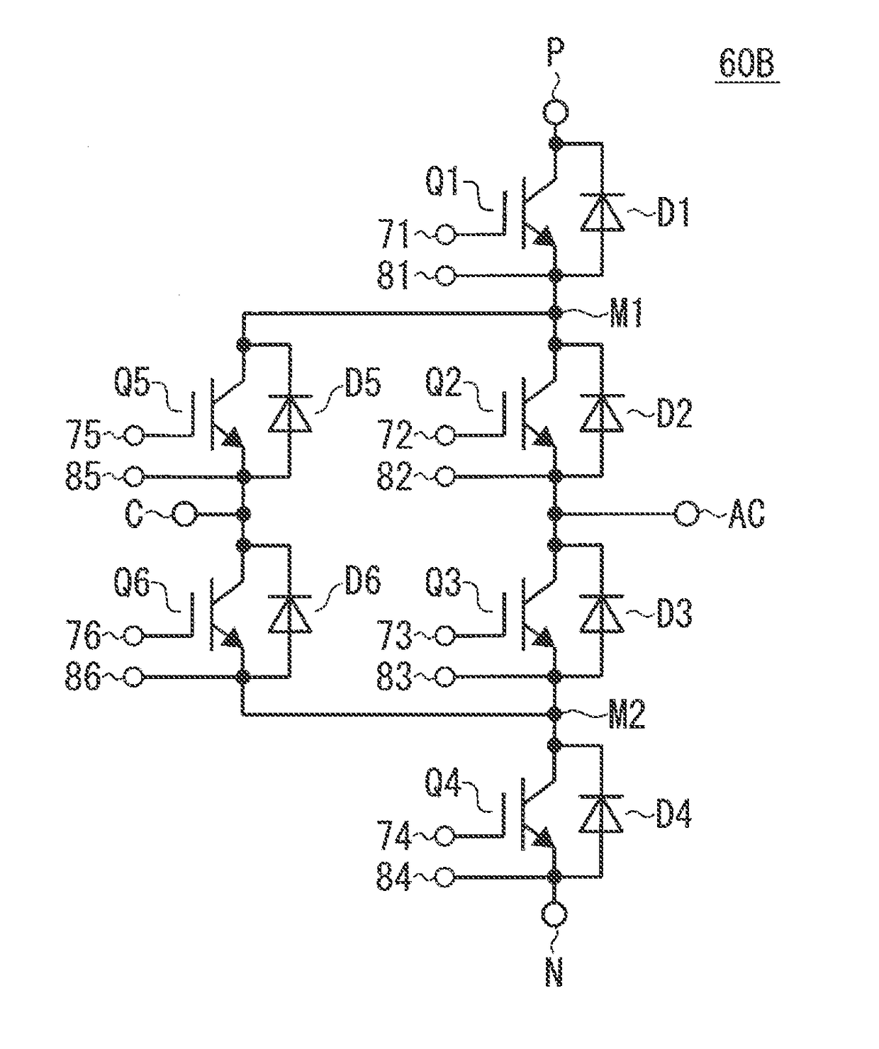
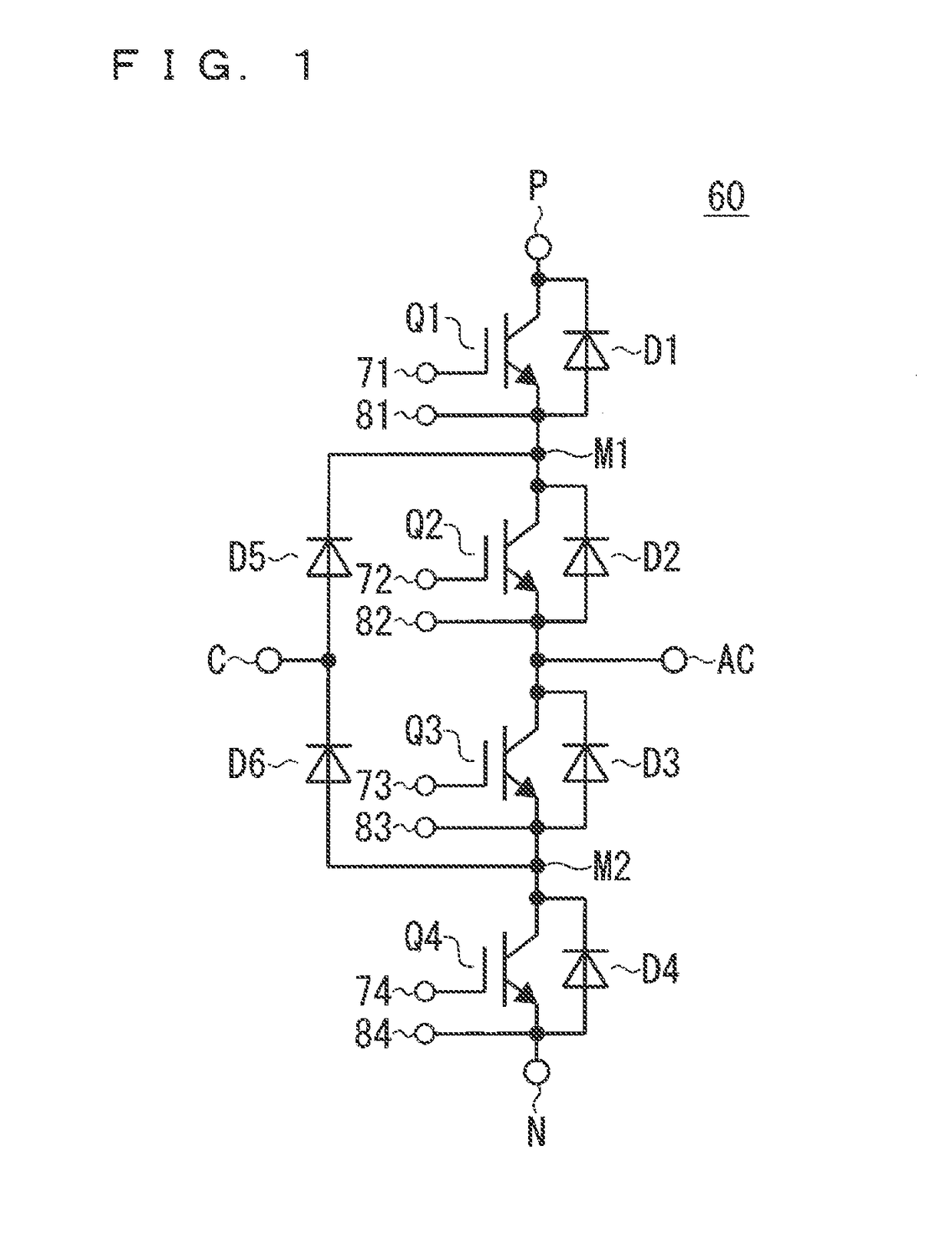
[0112]FIG. 7 is a circuit diagram showing module allocation substances of the invention of the present application which realizes the inverter circuit 60 shown in FIG. 1 by using the power semiconductor modules 101 to 103 shown inFIG. 3 to FIG. 5.

[0113]As shown in this diagram, the circuit is separated into: a partial circuit part 20A including the transistor Q1, the diode D1, and the diode D5; a partial circuit part 20B including the transistor Q4 and the diodes D4 and D6; and a partial circuit part 20C including the transistors Q2 and Q3 and the diodes D2 and D3; and three power semiconductor modules 101 are allocated for the partial circuit parts 20A to 20C. Hereinafter, the allocation substances will be described in detail.

[0114]Regarding the partial circuit part 20A, the transistor Tr1 of the power semiconductor module 101 or the power semiconductor module 102 is allocated to the transistor Q1, and the diodes Di1 and Di2 are allocated to the d...

second preferred embodiment

[0272]In the above described first preferred embodiment, when the four power semiconductor module devices 100A and the four power semiconductor module devices 100B are mixedly disposed, the 2-column disposition of the module device group 200AB1 and the module device group 200AB2 is employed. A second preferred embodiment employs a configuration in which the four power semiconductor module devices 100A and the four power semiconductor module devices 100B are disposed in a single column.

[0273]FIG. 23 is an explanatory diagram showing a planar configuration of the second preferred embodiment of an electric-power converting device of a case in which the electric-power converting device is realized by a 4-parallel configuration by using the power semiconductor module device 100 shown in FIG. 6.

[0274]A circuit configuration equivalent to the electric-power converting device shown in FIG. 23 is the configuration shown in FIG. 9 as well as the first and second comparative techniques and the...

third preferred embodiment

[0300]FIG. 24 is an explanatory diagram showing an application system, which is a third preferred embodiment. As shown in this diagram, an electric-power converting device 400 is provided in an application system 300. A specific configuration of the electric-power converting device 400 corresponds to the electric-power converting device of the first preferred embodiment shown in FIG. 11 or the electric-power converting device of the second preferred embodiment shown in FIG. 23.

[0301]The application system 300 of the third preferred embodiment has, in the interior thereof, the electric-power converting device 400, thereby exerting the effects of small circuit inductance, a snubber-circuit-less system, downsizing and low cost, low loss, and expansion of operation ranges in relation to the electric-power converting device 400 in the interior.

First Mode

[0302]As a first mode of the application system 300, there is a mode in which a solar power conditioner system is constituted. In the so...


PUM


Abstract

An electric-power converting device having an inverter circuit of a 4-parallel configuration is realized by a combination of four first to third power semiconductor module devices. In each of module device groups, a single unit of the first power semiconductor module device and a single unit of the second power semiconductor module device are mixedly disposed so as to be alternately disposed. Furthermore, the first to third power semiconductor module devices have circuit element groups which have a common point that each circuit element group includes at least one of first and second transistors and first and second diodes.

Description

BACKGROUND OF THE INVENTIONField of the Invention[0001]The present invention relates to an electric-power converting device constituted by connecting a plurality of semiconductor modules typified by power semiconductor modules in parallel.Description of the Background Art[0002]In inverter circuit devices which are application systems, demands for higher voltages and lower loss are increased, and demands for inverter circuits having a 3-level I-type inverter configuration are increasing. Under such circumstances, the above described inverter circuit is formed by connecting a plurality of power semiconductor modules having a 2-in-1 configuration in parallel.[0003]Examples of the conventional technique which has realized the 3-level I-type inverter by using the power semiconductor modules having the 2-in-1 configuration include a 3-level electric-power converting device disclosed in Japanese Patent Application Laid-Open No. 2013-59248.[0004]The conventional 3-level electric-power conve...

Claims


Application Information

Patent Timeline
IPC IPC(8): H02J3/38H02M7/493H02M7/487F03D7/02H01L31/02G05F1/67
CPCH02J3/385G05F1/67F03D7/0284H02J3/386H02M7/493H01L31/02021H02M7/487H02M7/48H02M1/0038H02M7/003Y02E10/56Y02E10/72Y02E10/76
Inventor NISHIDA, NOBUYA
Owner MITSUBISHI ELECTRIC CORP
Why Eureka
Try Eureka