Carbon nanotube-based multi-sensor

a multi-sensor and carbon nanotube technology, applied in the field of carbon nanotube-based multi-sensors, can solve the problems of low sensitivity, lack of positioning flexibility, incompatibility with existing micro-electronic processes,

Active Publication Date: 2018-08-16
IBM CORP
View PDF0 Cites 5 Cited by
  • Summary
  • Abstract
  • Description
  • Claims
  • Application Information

AI Technical Summary

Benefits of technology

The present invention is about a carbon nanotube-based multi-sensor that can measure temperature, strain, and humidity in a chip package. The multi-sensor consists of a layer of carbon nanotube dispersion spray coated onto a chip and a laminate, which is then dried. A composite material is formed by patterning the carbon nanotube mesh and attaching metal electrodes to its terminal ends. The multi-sensor is placed within a microelectronic package and connected to electrical circuits on a laminate substrate. A processor is used to measure the variation in electrical properties at a defined frequency as a function of temperature, strain, and humidity. The technical effect of the invention is the ability to accurately measure important environmental factors that can impact the performance and reliability of microelectronic devices.

Problems solved by technology

However, disadvantages like size, low sensitivity, lack of positioning flexibility and / or incompatibility with existing micro-electronic processes limit their use especially for in-situ measurements in micro-electronic modules.

Method used


Image

  • Carbon nanotube-based multi-sensor
  • Carbon nanotube-based multi-sensor
  • Carbon nanotube-based multi-sensor

Examples


Embodiment Construction

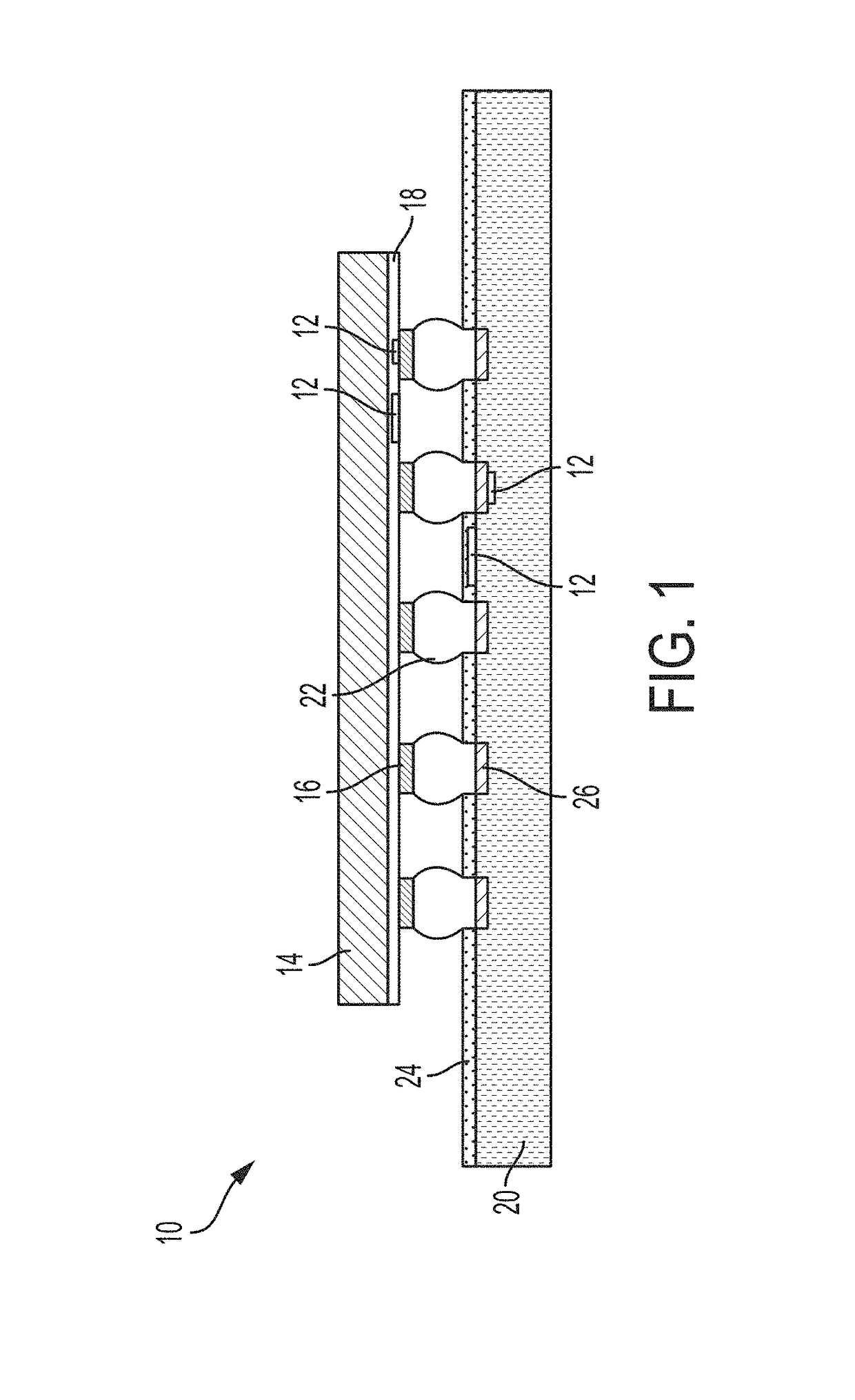
[0039]In high-performance semiconductors, the back-end-of-line (BEOL) interconnect pitch has been shrinking for decades following Moore's law. Steady advances in very-large-scale integration (VLSI) technology for both digital and analog devices could never have been achieved without overcoming various reliability risks in IC chips as well as packages. In many cases, such challenges do not reside solely in a package or an IC chip. Rather, the interaction between the package and the IC chip is important as the coefficients of thermal expansion (CTEs) of the silicon die and package materials, such as plastic molding compounds or organic substrates, can differ significantly. This CTE mismatch induces thermo-mechanical stresses at the interfaces during thermal excursions, which can compromise the chip's structural integrity. The influence of the package-induced stress on the chip is called chip-package interaction (CPI), and it plays a key role in overall product reliability. Similarly, ...


PUM

PropertyMeasurementUnit
RHaaaaaaaaaa
frequencyaaaaaaaaaa
frequencyaaaaaaaaaa

Abstract

Carbon nanotube-based multi-sensors for packaging applications and methods to form the carbon nanotube-based multi-sensors are capable of simultaneously measuring at least two measurands including temperature, strain, and humidity via changes in its electrical properties.

Description

DOMESTIC PRIORITY[0001]This application is a CONTINUATION of U.S. application Ser. No. 15 / 434,230, filed Feb. 16, 2017, the contents of which are incorporated by reference herein in its entirety.BACKGROUND[0002]The present invention relates to carbon nanotube-based multi-sensors, and more particularly, combined high sensitivity strain, temperature and / or humidity multi-sensors based on carbon nanotubes for microelectronic applications.[0003]A chip typically includes integrated circuits formed by front-end-of-line (FEOL) processing and metallization levels of an interconnect structure formed by back-end-of line (BEOL) processing. The chips are packaged in modules and usually not directly mounted on a circuit board. Module packaging provides electrical connectivity between the chip and the circuit board, protection against thermal and mechanical stresses, and protection against environmental corrosion. Solder bumps are commonly utilized to provide mechanical and electrical connections...

Claims


Application Information

Patent Timeline
Patent Type & Authority Applications(United States)
IPC IPC(8): G01N27/12G01K7/16G01L1/22H01L23/498H01L23/29H01L23/00
CPCH01L2224/16225G01K7/16G01L1/225G01N27/121H01L23/49811H01L23/293H01L24/16G01N27/127G01K7/226G01K2211/00G01L1/2287H01L23/3114H01L2224/0401H01L2224/13147H01L2924/1433H01L2924/1434H01L2224/131H01L2224/16237H01L2224/94H01L2224/73204H01L2224/32225H01L2224/92125H01L24/13H01L24/32H01L24/73H01L24/92H01L2924/00014H01L2924/014H01L2224/11H01L2924/00
Inventor DUCHESNE, ERICDROUIN, DOMINIQUEFREMONT, HELENELANDRY, SIMONQUELENNEC, AURORE F.M.E.SHAFIQUE, UMARWILSON, PATRICK R.J.
Owner IBM CORP
Why Eureka
Try Eureka