Activation Of Wafer Particle Defects For Spectroscopic Composition Analysis

a technology of composition analysis and active wafer particles, applied in semiconductor/solid-state device testing/measurement, material analysis, instruments, etc., can solve the problems of high volume production environment, inability to positively identify defect types and origins, and high cost of time, so as to enhance weak spectroscopic signatures and enhance electromagnetic fields

Active Publication Date: 2018-08-02
KLA TENCOR TECH CORP
View PDF3 Cites 7 Cited by
  • Summary
  • Abstract
  • Description
  • Claims
  • Application Information

AI Technical Summary

Benefits of technology

[0025]In some embodiments, multiple, different wavelengths are employed and the wavelengths are selected because they are known to interact with surface asperities of the substrate wafer (e.g., thin films, high aspect ratio protrusions of highly non-spherical defect particles, etc.). The surface asperities produce enhanced electromagnetic fields in their immediate vicinity that enhance weak spectroscopic signatures.

Problems solved by technology

However, in many cases defect images alone do not positively identify defect types and origins.
However, it is a time consuming process to obtain composition measurement results in high volume production environments, where review of patterned wafers by SEM and EDX tools is typically prioritized ahead of review of unpatterned wafers.
In addition, review by SEM and EDX tools that are separate from the particle defect review tool requires movement of the wafer from one tool to another, which costs time.
Although atomic vibrational bands of some particles can be observed with laser Raman microspectroscopy, in general, there are many important defect particles of interest (i.e., materials of interest) that do not exhibit active Raman vibrational bands, and are thus unobservable by Raman spectroscopic techniques.

Method used


Image

  • Activation Of Wafer Particle Defects For Spectroscopic Composition Analysis
  • Activation Of Wafer Particle Defects For Spectroscopic Composition Analysis
  • Activation Of Wafer Particle Defects For Spectroscopic Composition Analysis

Examples


Embodiment Construction

[0037]Reference will now be made in detail to background examples and some embodiments of the invention, examples of which are illustrated in the accompanying drawings.

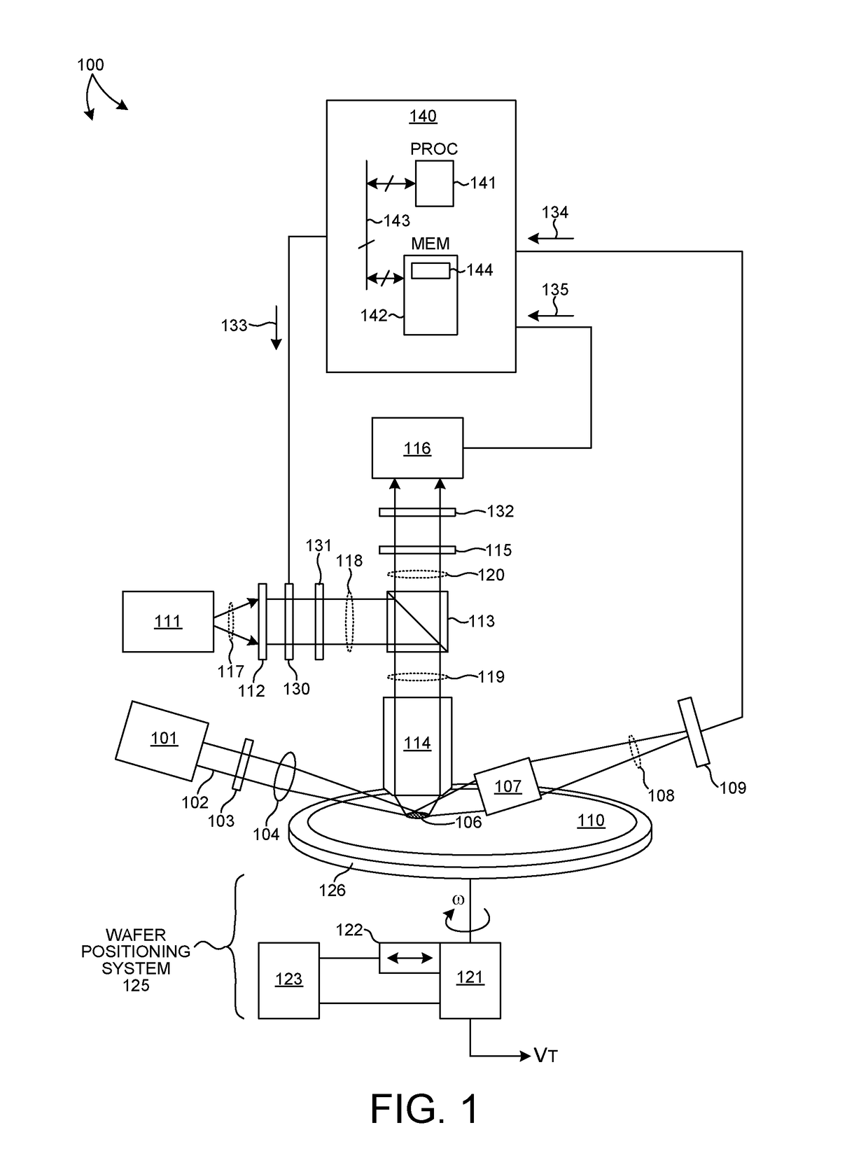
[0038]Methods and systems for detecting a particle defect on a wafer surface, transforming the particle to a spectroscopically active state, and identifying a material composition of the activated particle by a spectroscopic technique are described herein.

[0039]The inventive concepts described herein are based on the observation that many defect particles generated by semiconductor manufacturing equipment and processes are spectroscopically inactive (e.g., particles do not have atomic vibrational bands that can be observed with Raman spectroscopy). However, by chemical treatment, thermal treatment, photochemical treatment, or a combination thereof, particle defects are transformed such that an activated particle exhibits atomic vibrational bands that can be observed spectroscopically (e.g., via Raman spectroscopy).

[00...


PUM

PropertyMeasurementUnit
wavelength rangeaaaaaaaaaa

Abstract

Methods and systems for detecting a particle defect on a wafer surface, transforming the particle to a spectroscopically active state, and identifying a material composition of the activated particle by a spectroscopic technique are described herein. Particle defects are transformed by chemical treatment, thermal treatment, photochemical treatment, or a combination thereof, such that an activated particle exhibits atomic vibrational bands that can be observed spectroscopically. In one embodiment, a surface inspection system detects the presence of a particle defect on a wafer surface, activates observable Raman bands in one or more of the detected particles, and identifies the material composition of the activated particle by a spectroscopic technique. By performing both defect detection and composition analysis on the same inspection tool, it is not necessary to transfer a wafer to a different review tool, or combination of tools, to perform composition analysis of particle defects deposited on semiconductor wafers.

Description

TECHNICAL FIELD[0001]The described embodiments relate to systems for surface inspection, and more particularly to semiconductor wafer inspection modalities.BACKGROUND INFORMATION[0002]Semiconductor devices such as logic and memory devices are typically fabricated by a sequence of processing steps applied to a substrate or wafer. The various features and multiple structural levels of the semiconductor devices are formed by these processing steps. For example, lithography among others is one semiconductor fabrication process that involves generating a pattern on a semiconductor wafer. Additional examples of semiconductor fabrication processes include, but are not limited to, chemical-mechanical polishing, etch, deposition, and ion implantation. Multiple semiconductor devices may be fabricated on a single semiconductor wafer and then separated into individual semiconductor devices.[0003]Inspection processes are used at various steps during a semiconductor manufacturing process to detec...

Claims


Application Information

Patent Timeline
Patent Type & Authority Applications(United States)
IPC IPC(8): G01N21/65G01N21/95G01N21/94
CPCG01N21/65G01N2201/06113G01N21/94G01N21/9501H01L22/30H01L22/12H01L22/24
Inventor HALLER, KURT L.
Owner KLA TENCOR TECH CORP
Why Eureka
Try Eureka