
Photoelectric conversion element and solid-state imaging device

a conversion element and photoelectric technology, applied in the direction of solid-state devices, semiconductor devices, radiation controlled devices, etc., can solve the problems of deterioration of other characteristics, achieve the effect of improving responsivity, improving electric charge transport efficiency, and improving hole mobility and electron mobility

Active Publication Date: 2018-05-31
SONY SEMICON SOLUTIONS CORP
View PDF0 Cites 15 Cited by
  • Summary
  • Abstract
  • Description
  • Claims
  • Application Information

AI Technical Summary

Benefits of technology

The patent describes a photoelectric conversion element and a solid-state imaging device that have a superior spectroscopic shape, high responsivity, and high external quantum efficiency. The element is formed using three different organic semiconductor materials that improve hole and electron mobility while maintaining a sharp spectroscopic shape. This results in improved responsivity and external quantum efficiency, allowing for better image quality and performance. Overall, the patent provides a solution for creating a high-quality photoelectric conversion element and solid-state imaging device.

Problems solved by technology

However, in a case where one or two characteristics of the spectroscopic shape, responsivity, and EQE are improved, there is an issue that the other characteristics are deteriorated.

Method used


Image

  • Photoelectric conversion element and solid-state imaging device
  • Photoelectric conversion element and solid-state imaging device
  • Photoelectric conversion element and solid-state imaging device

Examples


application examples

2. Application Examples

Application Example 1

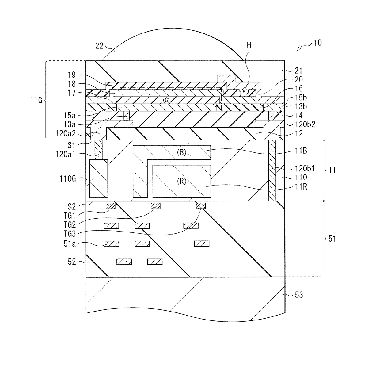
[0115]FIG. 10 illustrates an entire configuration of a solid-state imaging device (the solid-state imaging device 1) using the photoelectric conversion element 10 described in the foregoing embodiment as the unit pixel P. The solid-state imaging device 1 is a CMOS image sensor, and includes a pixel section 1a as an imaging region and a peripheral circuit section 130 in a peripheral region of the pixel section 1a on the semiconductor substrate 11. The peripheral circuit section 130 includes, for example, a row scanning section 131, a horizontal selection section 133, a column scanning section 134, and a system controller 132.

[0116]The pixel section 1a includes, for example, a plurality of unit pixels P (each corresponding to the photoelectric conversion element 10) that are two-dimensionally arranged in rows and columns. The unit pixels P are wired with pixel driving lines Lread (specifically, row selection lines and reset control lines) fo...

application example 2

[0121]The foregoing solid-state imaging device 1 is applicable to various kinds of electronic apparatuses having imaging functions. Examples of the electronic apparatuses include camera systems such as digital still cameras and video cameras, and mobile phones having imaging functions. FIG. 11 illustrates, for purpose of an example, a schematic configuration of an electronic apparatus 2 (e.g., a camera). The electronic apparatus 2 is, for example, a video camera that allows for shooting of a still image or a moving image. The electronic apparatus 2 includes the solid-state imaging device 1, an optical system (e.g., an optical lens) 310, a shutter unit 311, a driver 313, and a signal processor 312. The driver 313 drives the solid-state imaging device 1 and the shutter unit 311.

[0122]The optical system 310 guides image light (i.e., incident light) from an object toward the pixel section 1a of the solid-state imaging device 1. The optical system 310 may include a plurality of optical l...

experiment 1

f Spectroscopic Characteristics

[0124]A glass substrate was cleaned by UV / ozone treatment. Quinacridone (QD; the formula (3-1)) was evaporated on the glass substrate by a resistance heating method in a vacuum of 1×10⁻⁵ Pa or less with use of an organic evaporation apparatus while rotating a substrate holder. Evaporation speed was 0.1 nm / sec, and a film having a total thickness of 50 nm was formed as a sample 1. In addition, in place of using QD, a sample 2 using SubPcCl (the formula (6-1)), a sample 3 using C60 (the formula (1-1)), a sample 4 using αNPD (the formula (4-2)), a sample 5 using BTBT (the formula (5-1)), a sample 59 using BQD (the formula (3-2)), and a sample 60 using rubrene (the formula (8)) were fabricated, and spectroscopic characteristics of the respective samples were evaluated.

[0125]Transmittance and reflectivity for each wavelength were measured with use of an ultraviolet-visible spectrophotometer to determine absorptivity (%) of light absorbed by each of single-l...


PUM


Abstract

A photoelectric conversion element according to an embodiment of the present disclosure includes: a first electrode and a second electrode facing each other; and a photoelectric conversion layer provided between the first electrode and the second electrode, and including a first organic semiconductor material, a second organic semiconductor material, and a third organic semiconductor material that have mother skeletons different from one another. The first organic semiconductor material is one of fullerenes and fullerene derivatives. The second organic semiconductor material in a form of a single-layer film has a higher linear absorption coefficient of a maximal light absorption wavelength in a visible light region than a single-layer film of the first organic semiconductor material and a single-layer film of the third organic semiconductor material. The third organic semiconductor material has a value equal to or higher than a HOMO level of the second organic semiconductor material.

Description

TECHNICAL FIELD[0001]The present disclosure relates to a photoelectric conversion element using, for example, an organic semiconductor and a solid-state imaging device including the same.BACKGROUND ART[0002]In recent years, in solid-state imaging devices such as CCD (Charge Coupled Device) image sensors and CMOS (Complementary Metal Oxide Semiconductor) image sensors, reduction in pixel size has accelerated. The reduction in pixel size reduces the number of photons entering a unit pixel, which results in reduction in sensitivity and reduction in S / N ratio. Moreover, in a case where a color filter including a two-dimensional array of primary-color filters of red, green, and blue is used for colorization, in a red pixel, green light and blue light are absorbed by the color filter, which causes reduction in sensitivity. Further, in order to generate each color signal, interpolation of pixels is performed, which causes so-called false color.[0003]Accordingly, for example, PTL 1 disclose...

Claims


Application Information

Patent Timeline
Patent Type & Authority Applications(United States)
IPC IPC(8): H01L27/30H01L27/28H01L51/42H01L51/00
CPCH01L27/307H01L27/286H01L51/4273H01L51/0046H01L51/0047H01L51/008H01L51/0072H01L51/006H01L51/0059H01L51/0074H01L51/0054H01L51/001H01L51/0058H01L27/14647H01L27/14689H10K39/32H10K85/211H10K30/30H10K85/322H01L27/146H01L31/10Y02E10/549H10K85/215H10K85/622H10K85/626H10K85/633H10K85/6572H10K85/6576H10K30/81H01L27/14643H10K85/657H10K2101/30H10K19/20H10K30/353H10K71/164H10K85/631
Inventor HASEGAWA, YUTAMATSUZAWA, NOBUYUKIOBANA, YOSHIAKITAKEMURA, ICHIRONAKAYAMA, NORIKAZUSHIMOKAWA, MASAMIYAMAGUCHI, TETSUJIYAGI, IWAOMOGI, HIDEAKI
Owner SONY SEMICON SOLUTIONS CORP
Learn More