Integrated Passive Device for RF Power Amplifier Package

a passive device and power amplifier technology, applied in the field of radio frequency (rf) power amplifier packages, can solve the problems of biasing of transistors, increasing the amplitude of undesired signal components, and the large output capacitance of most rf power transistors, so as to achieve less space, less space, and limited space inside the package

Active Publication Date: 2018-01-25
AMPLEON NETHERLANDS
View PDF0 Cites 2 Cited by
  • Summary
  • Abstract
  • Description
  • Claims
  • Application Information

AI Technical Summary

Benefits of technology

The patent text describes a new technique for improving the control of impedance in electronic circuits. This technique involves shifting the first resonance frequency to lower frequencies and using a second resonance frequency to better control the impedance at frequencies associated with the second order modulation. The text also mentions using a bias lead and a fourth plurality of bond wires to eliminate the need for an Lfeed and reduce space on the external printed circuit board. The technical effect of this patent is improved control of impedance and reduced space requirements on printed circuit boards.

Problems solved by technology

If the impedance seen by an RF power transistor at these frequencies is too high, the amplitude of the undesired signal components may increase, and the biasing of the transistor may be affected by feedback of the low-frequency IMD products into the biasing circuitry.
In practice however, most RF power transistors may have a considerable output capacitance.

Method used


Image

  • Integrated Passive Device for RF Power Amplifier Package
  • Integrated Passive Device for RF Power Amplifier Package
  • Integrated Passive Device for RF Power Amplifier Package

Examples


Embodiment Construction

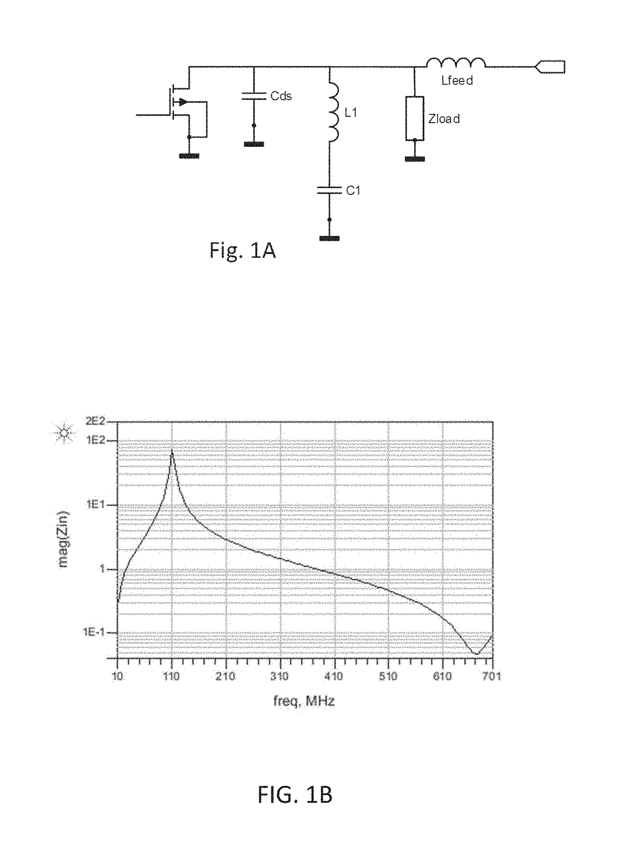
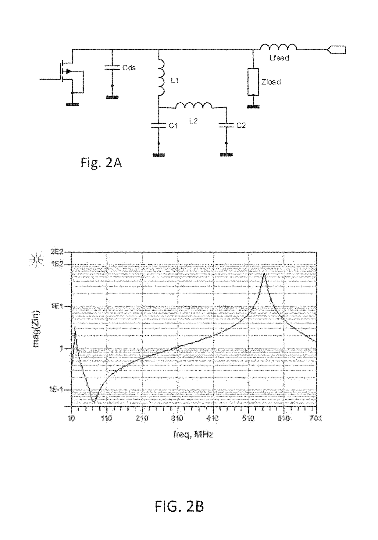
[0055]FIG. 3A illustrates a general topology in accordance with the present disclosure.

[0056]When comparing this topology with the topology in FIG. 2A, it can be seen that C1 is no longer directly connected to ground but is instead connected to C2. This latter capacitor, being substantially larger than C1, may act as a ground at the operational frequency of the RF power transistor. In addition, a resistive element R is arranged in series with L2.

[0057]Similar to the topology of FIG. 2A, a first resonance can be observed in the impedance seen looking away from the FET illustrated in FIG. 3B, which can be attributed to the parallel resonance of C2 and Lfeed. At this resonance frequency, the impedance of the series connection of L2 and R may be substantially smaller than the impedance of C1. As such, the effective capacitance that is arranged in parallel to Lfeed may be roughly equal to C2. Moreover, the currents at this frequency may flow through R, causing damping of the resonance pe...


PUM


Abstract

The present disclosure relates to a radio frequency (RF) power transistor package. It further relates to a mobile telecommunications base station comprising such an RF power transistor package, and to an integrated passive die suitable for use in an RF power amplifier package. In example embodiments, an in-package impedance network is used that is connected to an output of the RF power transistor arranged inside the package. This network comprises a first inductive element having a first and second terminal, the first terminal being electrically connected to the output of the RF transistor, a resonance unit electrically connected to the second terminal of the first inductive element, and a second capacitive element electrically connected in between the resonance unit and ground, where the first capacitive element is arranged in series with the second capacitive element.

Description

CROSS-REFERENCE TO RELATED APPLICATION[0001]The present application is a non-provisional patent application claiming priority to Netherlands Patent Application No. 2017206 filed Jul. 21, 2016, the contents of which are hereby incorporated by reference.TECHNICAL FIELD[0002]The present disclosure relates to a radio frequency (RF) power amplifier package. It further relates to a mobile telecommunications base station comprising such an RF power amplifier package, and to an integrated passive die suitable for such an RF power amplifier package.BACKGROUND[0003]RF power amplifier packages may comprise a package and a semiconductor die, and the die may be arranged inside the package and provided with an RF power transistor. The RF power transistor may have an output capacitance and may be configured to amplify signals at an operational frequency. An impedance network may be arranged inside the package for providing impedance matching and / or filtering. These packages may be used in base sta...

Claims


Application Information

Patent Timeline
IPC IPC(8): H03H7/38H01L23/00H03F3/195H03F1/02H03F1/32H01L23/66H03F3/24
CPCH01L23/66H03F2200/387H01L24/49H03F3/195H03F3/245H03F1/0288H03F1/3205H01L2223/6672H01L2223/6655H01L2924/19011H01L2224/48137H01L2224/49176H01L2924/19041H01L2924/19042H01L2924/19043H01L2924/19015H01L2924/19051H01L2924/19105H01L2924/10253H01L2924/1033H01L2924/13091H03F2200/451H01L24/48H03F1/565H03F3/189H03F2200/391H03F2200/399H03H7/1791H01L2924/00014H01L2224/45099H03H7/38
Inventor DE BOET, JOHANNES ADRIANUS MARIAVAN RIJS, FREERKSVESHTAROV, IORDAN KONSTANTINOV
Owner AMPLEON NETHERLANDS
Why Eureka
Try Eureka