
Stack type test interface board assembly and method for manufacturing the same

Inactive Publication Date: 2017-11-02
CHUNGHWA PRECISION TEST TECH
View PDF4 Cites 0 Cited by
  • Summary
  • Abstract
  • Description
  • Claims
  • Application Information

AI Technical Summary

Benefits of technology

The present invention provides a stack type test interface board assembly with the benefits of decreased manufacture time, reduced number of layers, increased yield, and increased transmission quality. The assembly achieves the divided stages of fan-out and fan-in through the use of through hole or blind hole, thus solving the problem of unstable characteristic impedance and improving the test of wirings with smaller width and space. Additionally, the assembled board is easy to repair and improve transmission efficiency.

Problems solved by technology

However, limited to the process capability, the deployments of power and GND reduced greatly, the quality of power integration (PI) gets worse.
Additionally, the deployments of the fan-out wirings are concentrated in 1-2 layers of the test loadboard structure, increasing the mutual interference of the signals between the wirings.

Method used


Image

  • Stack type test interface board assembly and method for manufacturing the same
  • Stack type test interface board assembly and method for manufacturing the same
  • Stack type test interface board assembly and method for manufacturing the same

Examples


second embodiment

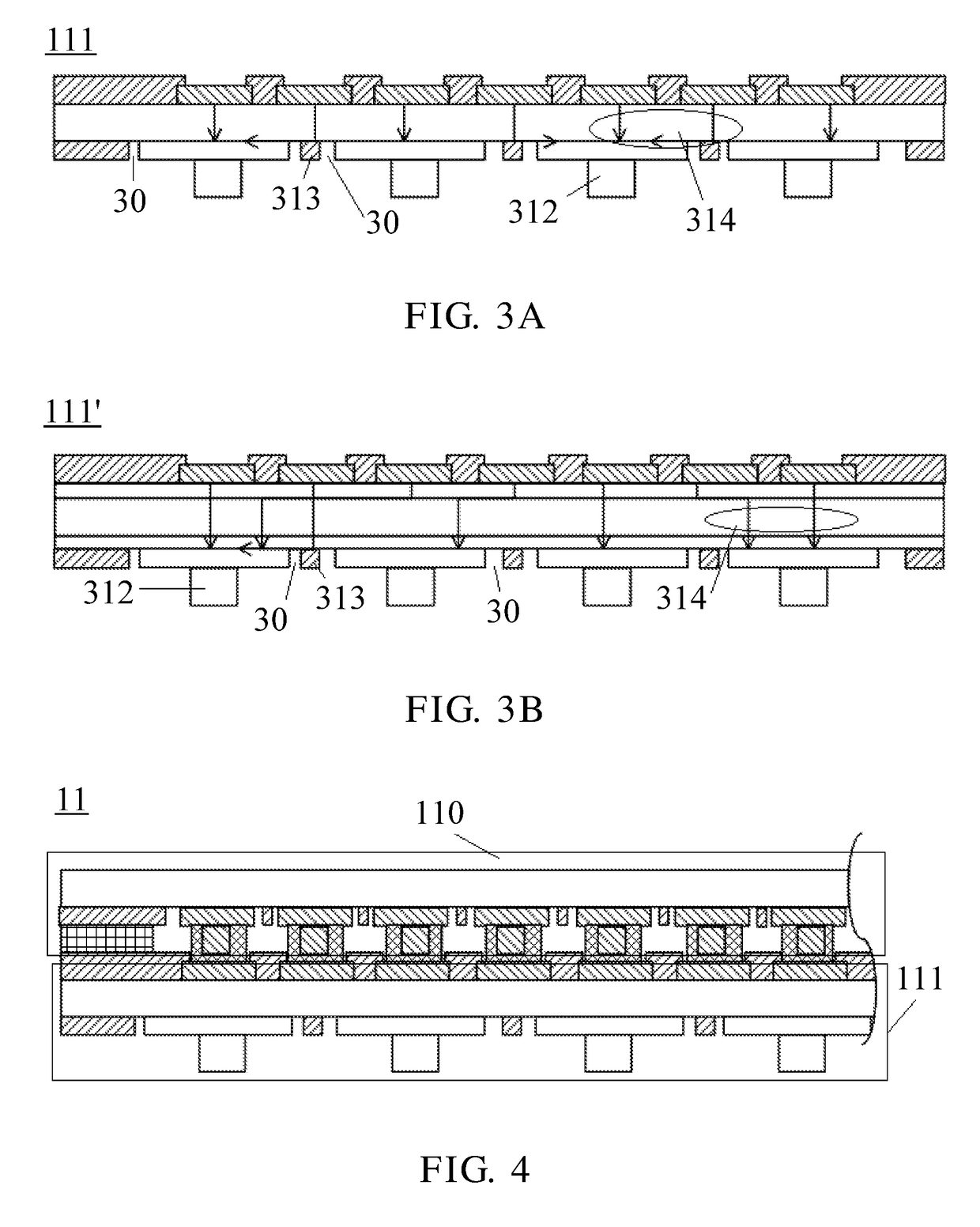
[0032]FIG. 3B shows a lateral-view diagram of the wide pitch transform board with a multi-layers structure, according to the present invention.

[0033]Preferably, each second connection node 312 is a metal bump. There is a compartment layer 313 formed between every two adjacent metal bumps, and as marked in FIGS. 3A and 3B, the arrow indicates a transmission path 314 of each metal bump in the wide pitch transform board 111.

[0034]Preferably, each aforementioned metal bump is a copper hump.

first embodiment

[0035]Please refer to FIG. 4 which illustrates a lateral-view diagram of an assembled space transform board according to the present invention. The space transform board 11 includes a narrow pitch transform board 110 and a wide pitch transform board 111, wherein a pad material 40 and solder paste 41 are intermediately disposed therebetween.

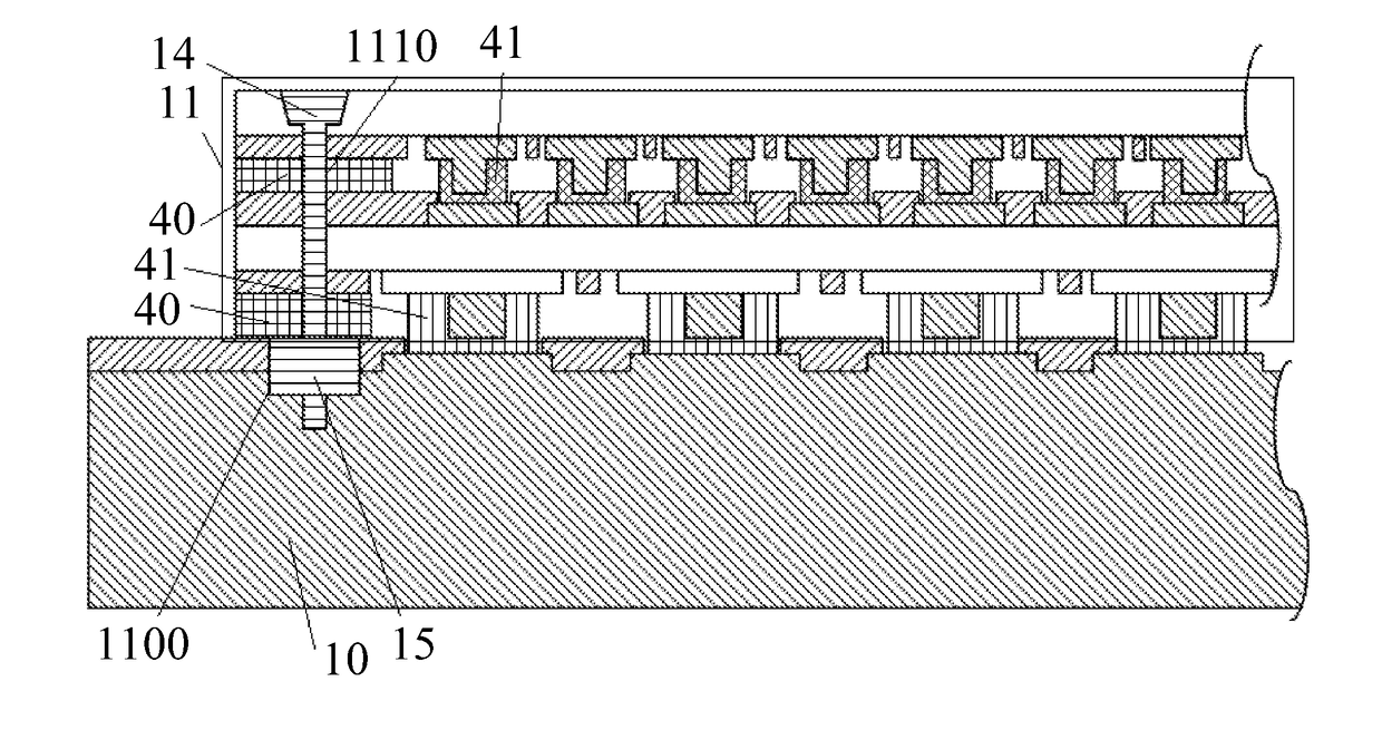
[0036]Please refer to FIG. 5 which illustrates a lateral-view diagram of assembled the stack type test interface board assembly, applied for a semi-finished semiconductor product which has not been packaged yet, according to the first embodiment of the present invention. Each of the second connection nodes 312 is welded to the weld pad on the side of the printed circuit board 10 to form an electrical connection therebetween. The printed circuit board 10 is realized as a probe card board, used for testing the semi-finished semiconductor product, and the other side of the probe card board 10 is used for electrically connecting to a test machine.

[003...


PUM


Abstract

A stack type test interface board assembly is provided herein, which comprises: a space transform board having a narrow pitch transform board and a wide pitch transform board, a plurality of first connection nodes disposed on a side of the narrow pitch transform board to be electrically connected to a finished or semi-finished semiconductor product, a plurality of second connection nodes disposed on a side of the wide pitch transform board, and a printed circuit board where a side thereof is electrically connected to the plurality of the second connection nodes. The narrow pitch transform board and the wide pitch transform board are assembled in perpendicular stack into the space transform board. A pitch between each two of the plurality of the first connection nodes is smaller than a pitch between each two of the plurality of the second connection nodes.

Description

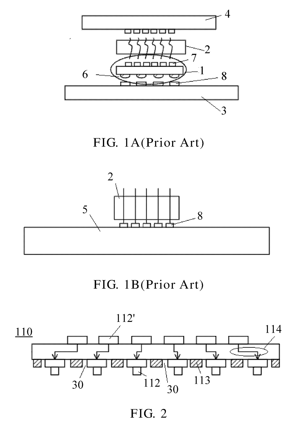
FIELD OF THE INVENTION[0001]The present invention relates to a test interface board assembly and a method for manufacturing the same, and in particular to a stack type test interface board assembly and a method for manufacturing the same.BACKGROUND OF THE INVENTION[0002]Please refer to FIGS. 1A and 1B. FIG. 1A illustrates a lateral-side diagram of a conventional test interface board assembly, which is generally adopted for a yield test of a semi-finished semiconductor product without being packaged, such as wafer 4. Such a test interface board assembly has a transform interface of different spaces (pitches) between the wafer and the test machine. For example, the main composition structure of the test interface board assembly includes an integrally-formed space transform (ST) board 1 having a space (pitch) between each two connecting nodes corresponding to I / O bumps of the tested wafer 4 in a narrower space specification, and a printed circuit board (PCB) 3 such as probe test loadbo...

Claims


Application Information

Patent Timeline
IPC IPC(8): G01R1/073H01L21/48G01R1/04
CPCG01R1/07378H01L21/4857G01R1/0491H01L21/4853H01L21/486
Inventor LIN, CHENG-JUEILI, WEN TSUNGTENG, YUAN - CHIANGHSIEH, KAI CHIEH
Owner CHUNGHWA PRECISION TEST TECH
Learn More