
Exposure method, method of fabricating periodic microstructure, method of fabricating grid polarizing element and exposure apparatus

a grid polarizing element and exposure apparatus technology, applied in the field of exposure methods, can solve the problems of two light beams interfering, and achieve the effects of reducing the number of shots, reducing the cost, and small siz

Active Publication Date: 2017-09-14
USHIO DENKI KK
View PDF11 Cites 2 Cited by
  • Summary
  • Abstract
  • Description
  • Claims
  • Application Information

AI Technical Summary

Benefits of technology

The present invention employs a so-called "step-and-repeat" type exposure method, which reduces the size of the apparatus and lowers the cost. In two-beam interference exposure, the interfering light irradiation regions in successive shots are exposed such that they are aligned with each other in the substrate conveying direction without overlapping. This reduces the number of shots required and improves throughput, resulting in higher processing efficiency and lower costs.

Problems solved by technology

The above mentioned two-beam interference exposure method branches light from a light source having a high coherency (interference), such as a laser or the like, into two light beams and causes the two light beams to interfere each other.

Method used


Image

  • Exposure method, method of fabricating periodic microstructure, method of fabricating grid polarizing element and exposure apparatus
  • Exposure method, method of fabricating periodic microstructure, method of fabricating grid polarizing element and exposure apparatus
  • Exposure method, method of fabricating periodic microstructure, method of fabricating grid polarizing element and exposure apparatus

Examples


first embodiment

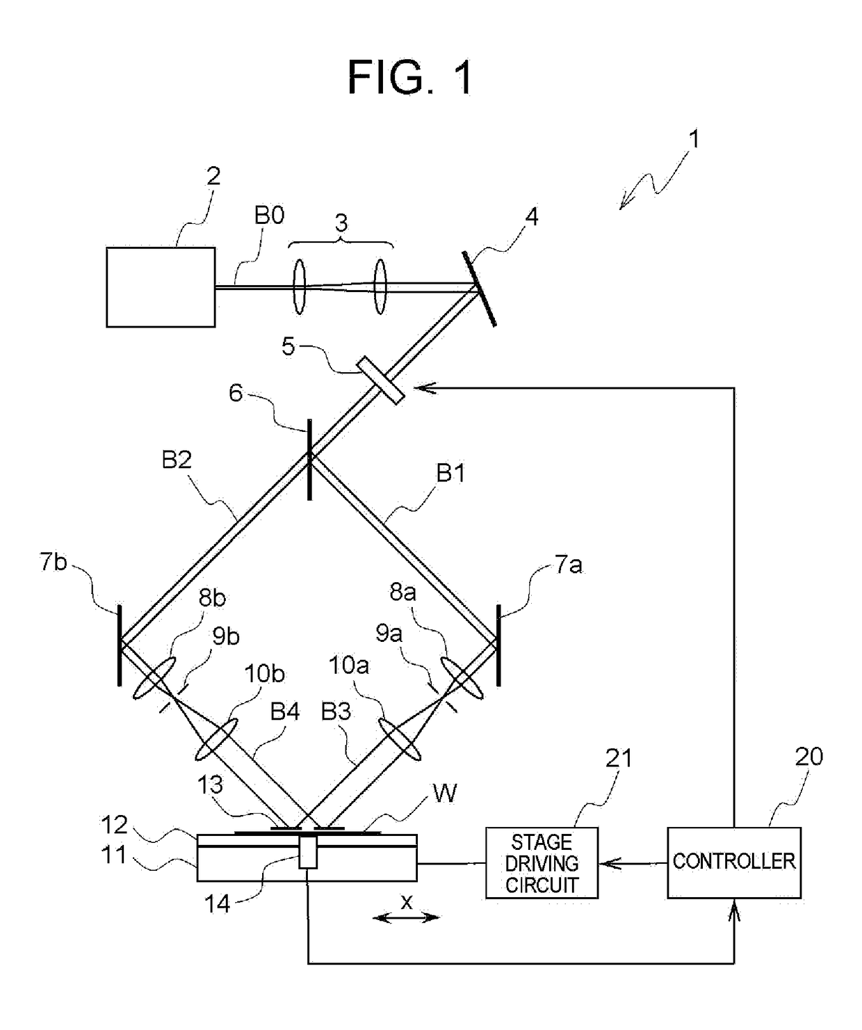
[0072]FIG. 1 is a view schematically showing an exemplary configuration of an exposure apparatus according to the present invention.

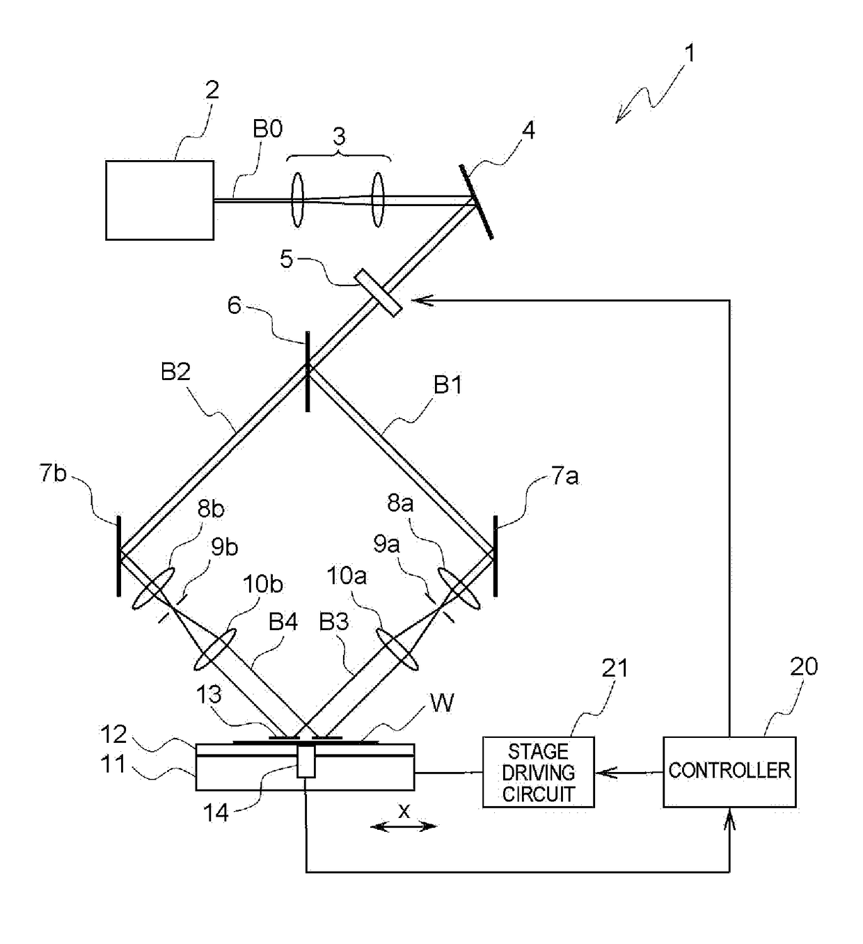
[0073]In FIG. 1, reference sign 1 denotes the exposure apparatus. The exposure apparatus is provided with a light source 2, a beam expander 3, a downwardly deflecting mirror 4; a shutter 5, a beam branching element 6, a reflecting (or folding) mirrors 7a and 7b, a light condensing (condenser) lenses 8a and 8b, pinholes 9a and 9b, and collimating lenses 10a and 10b. Furthermore, the exposure apparatus 1 may be provided with a stage 11, an adhesive disk 12, a mask 13, a gap sensor 14, a controller 20, and a stage driving circuit 21.

[0074]The light source 2 is a coherent light source which emits coherent light, and for example, a semiconductor excited (pumped) solid laser that emits the laser light having a wavelength λ of, for example, 266 nm. The beam diameter of the laser light B0, emitted from the light source 2, is expanded (enlarged) by the beam expa...

second embodiment

[0149]Hereinafter, a second embodiment of the present invention will be described below in detail.

[0150]In the above mentioned first embodiment, when the effective irradiation regions E0 are aligned with one another in the substrate conveying direction, the interfering regions E1 are not overlapped each other but the non-interfering regions E2 are overlapped each other. On the other hand, according to the second embodiment, the non-interfering region E2 is overlapped with the neighboring interfering region E1.

[0151]FIG. 14 is a view showing an exposure method according to the second embodiment.

[0152]As shown in FIG. 14A, the exposure apparatus 1 conveys the work W so as not to overlap the interfering region E1 in the effective irradiation region E0 at m-th exposure and the interfering region E1 in the effective irradiation region E0 at (m−1)-th exposure. Furthermore, according to the second embodiment, the exposure apparatus 1 conveys the work W so as to overlap the interfering regi...

third embodiment

[0157]Next, hereinafter, a third embodiment of the present invention will be described below in detail.

[0158]In the above mentioned first and second embodiments, the mask 13 is arranged above the workpiece W with the gap D being provided. On the other hand, according to the third embodiment, the mask 13 is arranged directly on the workpiece W without the gap D being provided.

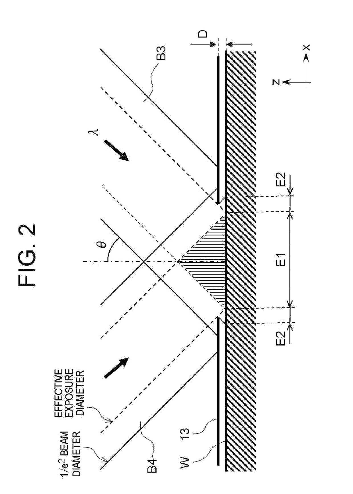
[0159]In the third embodiment, the exposure apparatus 1 performs the exposure in a state that the mask 13 is contacting the workpiece W. In this case, as the light beam is not wrapped around unlike those shown in FIG. 2, the non-interfering region E2 is not formed at both edges of the interfering region E1. In other words, the area of the effective irradiation region E0 is become equal to the area of the interfering region E1.

[0160]When exposing by the step-and-repeat method, as shown in FIG. 15, the exposure is to be performed so as not to overlap the neighboring interfering regions E1 (=the effective irradiati...


PUM

PropertyMeasurementUnit
wavelengthaaaaaaaaaa
sizeaaaaaaaaaa
photosensitive thresholdaaaaaaaaaa

Abstract

Disclosed herein an exposure apparatus capable of implementing a microfabrication onto a work with a higher throughput and a lower cost. The exposure apparatus generates interfering light by crossing two or more branched light beams branched from output light from a coherent light source at a predetermined interfering angle, and exposes the substrate by repeating an irradiation onto the substrate with the interfering light and a conveyance of the substrate. At this moment, the exposure apparatus shapes in interfering light irradiation region on the substrate onto which the interfering light is irradiated into a predetermined shape. Then, the exposure apparatus disposes a plurality of the interfering light irradiation regions in successive shots to be located adjacent to each other on the substrate in a direction of conveying the substrate without the interfering light irradiation regions being overlapped when exposing the substrate while conveying the substrate in a stepwise manner.

Description

FIELD OF THE INVENTION[0001]The present invention relates to an exposure method of implementing a fine periodic pattern on a substrate, a method of fabricating a periodic microstructure using the exposure method, a method of fabricating a grid polarizing element, and an exposure apparatus.DESCRIPTION OF THE RELATED ART[0002]Conventionally, as a method of implementing a microfabrication or a fine processing, the two-beam interference exposure method has been known. The two-beam interference exposure method herein is a method that causes two laser beams to cross each other at a predetermined angle to generate interfering (or coherent) light (i.e., an interference fringe or an interference stripe) that has a contrast (i.e., a light intensity distribution) at a pitch similar to or less than a wavelength of the laser beam, and to irradiate a substrate with the interfering light generated. The above mentioned two-beam interference exposure method branches light from a light source having ...

Claims


Application Information

Patent Timeline
Patent Type & Authority Applications(United States)
IPC IPC(8): G03F7/00
CPCG02B5/3058G03F7/0005G02B5/3075G03F7/201G03F7/203G03F7/22G03F7/70408G03F7/70475
Inventor YAJIMA, DAISUKENOMOTO, KENTARONAWAKI, YOHEI
Owner USHIO DENKI KK
Learn More