
Localized surface plasmon resonance sensing chip and localized surface plasmon resonance sensing system

a technology sensing chip, which is applied in the field of localized surface plasmon resonance sensing chip and localized surface plasmon resonance sensing system, can solve problems such as difficult measurement of spectra, and achieve the effect of high accuracy

Inactive Publication Date: 2017-08-03
NAT INST OF ADVANCED IND SCI & TECH
View PDF3 Cites 3 Cited by
  • Summary
  • Abstract
  • Description
  • Claims
  • Application Information

AI Technical Summary

Benefits of technology

The present invention provides a localized surface plasmon resonance sensing chip that can accurately measure changes in refractive index of a surface by measuring the peak wavelength shift of an optical spectrum. This chip has a narrow linewidth of the absorption spectrum, ensuring high accuracy in the measurement. The invention also includes a localized surface plasmon resonance sensing system using this chip for surface plasmon resonance sensing.

Problems solved by technology

However, since an absorption spectrum originating from localized plasmon resonance has a relatively broad linewidth, some contrivance is required for this chip to detect minute spectral shifts.
It is very difficult to measure spectra by using conventional tabletop-size spectral photometers at a bedside, a clinical site, an airport and a seaport, or a region without a sufficient social infrastructure.

Method used


Image

  • Localized surface plasmon resonance sensing chip and localized surface plasmon resonance sensing system
  • Localized surface plasmon resonance sensing chip and localized surface plasmon resonance sensing system
  • Localized surface plasmon resonance sensing chip and localized surface plasmon resonance sensing system

Examples


example

[0068](Refractive Index Response Sensitivity of Sensing Chip)

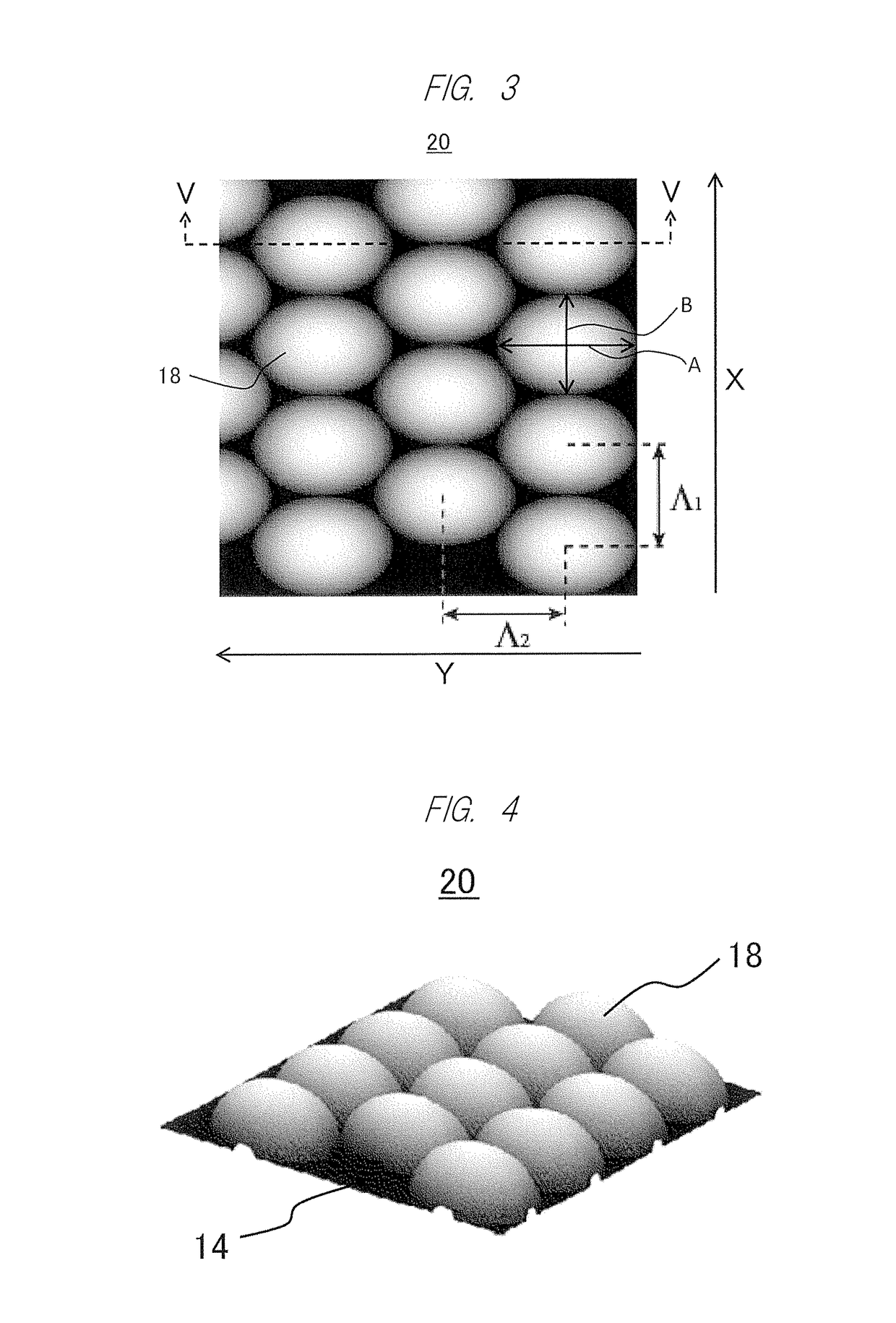
[0069]Absorbance of light transmitted through a sensing chip having a stretching degree L / L0 (corresponding to A / B in FIG. 3) of 1.2 before the formation of a metal layer on its front surface in each type of mediums was measured. A tabletop spectrophotometer (U-1900 manufactured by Hitachi High-Technologies Corporation) was used to measure absorbance spectra. FIG. 10 shows these optical spectra. When a refractive index n of the detection region surface of the sensing chip changed, the peak wavelength of an optical spectrum also greatly changed. FIG. 11 shows a relation between a refractive index n of a medium present on the detection region surface of the sensing chip and a peak wavelength of an optical spectrum. The refractive index response sensitivity being the gradient of the plot in FIG. 11 was about 440, which was twice or more the refractive index response sensitivity of the chip described in International Publicati...


PUM


Abstract

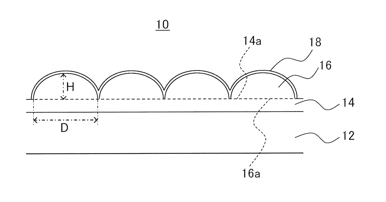
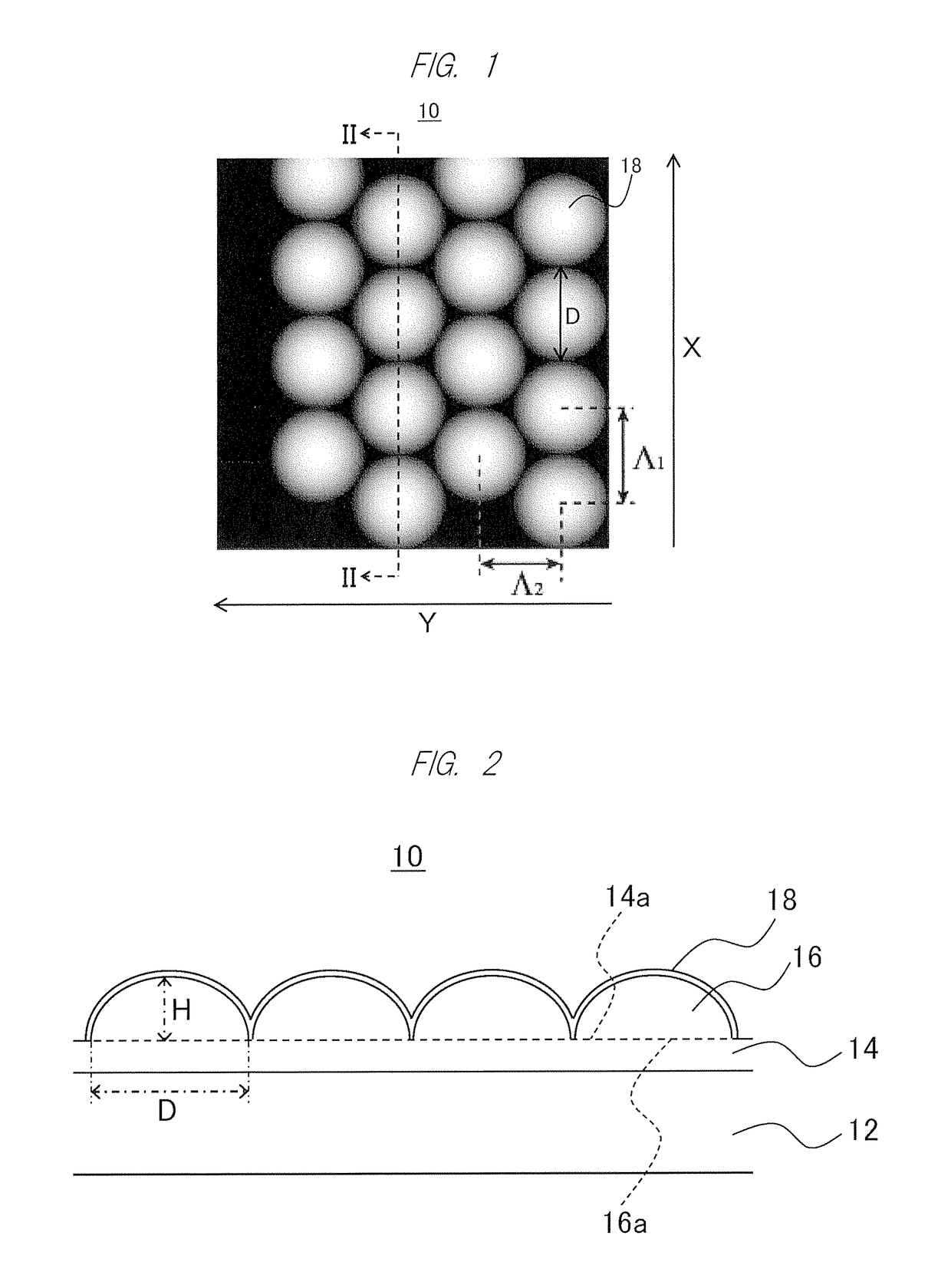
There are provided a localized surface plasmon resonance sensing chip in which a linewidth of an absorption spectrum originating from localized plasmon resonance is narrow and with which a peak wavelength shift of an optical spectrum accompanying a change in refractive index of a surface can be accurately measured, and a localized surface plasmon resonance sensing system using this sensing chip. A sensing chip 10 includes a base 14 having a flat-plate shape, a plurality of protruding portions 16, and a metal layer 18 covering each front surface of the plurality of protruding portions 16. The protruding portions 16 each have a shape like a semi-oblate spheroid which is one of three-dimensional parts obtained by dividing an oblate spheroid in half along an equatorial plane and are arranged such that a divided surface 16a of the semi-oblate spheroid faces a front surface 14a of the base 14. A sensing system includes the sensing chip 10, a light source irradiating a detection region of the sensing chip 10 with light, and a photodetector detecting the optical spectrum of light emitted from the light source and then reflected in or transmitted through the detection region of the sensing chip 10.

Description

CROSS-REFERENCE TO RELATED APPLICATION[0001]This application is a National Stage application of International Patent Application No. PCT / JP2015 / 071866, filed on Jul. 31, 2015, which claims priority to Japanese Patent Application Number 2014-158793, filed on Aug. 4, 2014, each of which is hereby incorporated by reference in its entirety.TECHNICAL FIELD[0002]The present invention relates to a highly sensitive sensing chip using localized surface plasmon resonance and a sensing system using this sensing chip.BACKGROUND ART[0003]A highly sensitive localized surface plasmon resonance sensor chip is known (International Publication No. WO 2011 / 121857). The chip described in International Publication No. WO 2011 / 121857 has higher sensitivity than conventional ones. However, since an absorption spectrum originating from localized plasmon resonance has a relatively broad linewidth, some contrivance is required for this chip to detect minute spectral shifts. For this reason, in some cases, th...

Claims


Application Information

Patent Timeline
IPC IPC(8): G01N21/552G02B5/00
CPCG02B5/008G01N21/554G01N21/55G01N21/553
Inventor FUKUDA, TAKASHIEMOTO, AKIRA
Owner NAT INST OF ADVANCED IND SCI & TECH
Learn More