
A high dynamic range pixel and a method for operating it

Active Publication Date: 2017-07-27
SONY DEPTHSENSING SOLUTIONS SA NV
View PDF4 Cites 13 Cited by
  • Summary
  • Abstract
  • Description
  • Claims
  • Application Information

AI Technical Summary

Benefits of technology

The present invention relates to a method for accurate time-of-flight applications. The method provides consistent datasets without the need for calibration between different conversion gains, which is a big advantage compared to other methods. This allows for easier and more accurate timing information to be collected. The technical effect of the method is improved accuracy and efficiency in time-of-flight applications.

Problems solved by technology

This is not possible when using a standard one-mode capacitance.

Method used


Image

  • A high dynamic range pixel and a method for operating it
  • A high dynamic range pixel and a method for operating it
  • A high dynamic range pixel and a method for operating it

Examples


Embodiment Construction

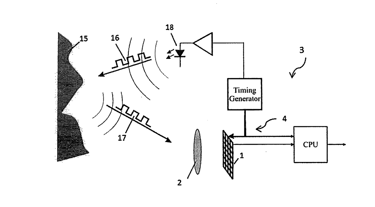
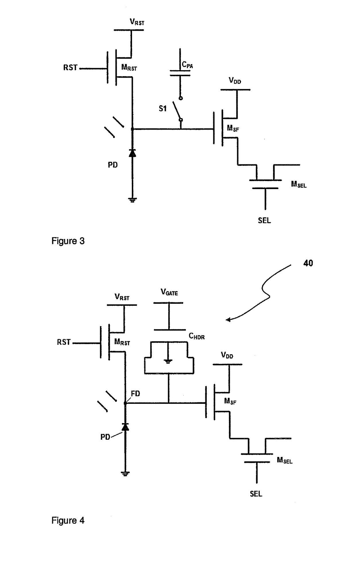
[0035]FIG. 4 illustrates a pixel configuration according to an embodiment of the invention.

[0036]The pixel 40 comprises:[0037]a photosensitive element PD, for instance a photodiode, for generating charges in response to impinging light; a pinned photodiode could be used also;[0038]a detector node FD, which is the node attached to the cathode of the photodiode in case there is no transfer gate, or a detector node FD which can be connected to the PD element by means of a transfer gate, not represented;[0039]a reset transistor MRST responsive to a control signal RST and operable to initialise the photosensitive element PD to a known voltage (VRST), or to reset the element FD to a known voltage while depleting completely the pinned photodiode, if a pinned photodiode is used;[0040]an amplifier transistor MSF, for instance a source-follower, responsive to a VDD signal and operable to allow the pixel voltage to be observed without removing the accumulated charge; the voltage at the detecto...


PUM


Abstract

The invention relates to a HDR pixel comprising a photo-sensitive element; a detector node connected to the photo-sensitive element; a reset switch connected to the detector node for resetting the detector node to a predetermined voltage; a buffer amplifier having an input connected to the detector node; a selecting transistor operable to select said pixel during a read out process; an intrinsic parasitic capacitance originated from at least one of the photo-sensitive element, the detector node, the reset switch, the buffer amplifier, the selecting transistor and operable to store the minority carriers generated by the photo-sensitive element; characterized in that the pixel further comprises a dual-mode capacitance having an input connected to the detector node and being operable in storing and destoring modes, for storing the generated minority carriers while being in the storing mode and destoring the minority carriers into the parasitic capacitance, while being in the destoring mode.

Description

TECHNICAL FIELD OF THE INVENTION[0001]The invention relates to a High-Dynamic-Range (HDR) pixel and to a method for operating it. More particularly, the invention relates to a HDR pixel for performing Time-Of-Flight measurements and enabling to use different conversion gains, without destroying the charge information.BACKGROUND OF THE INVENTION[0002]An image sensor is a device capturing and converting an impinging electromagnetic radiation such as a light flux into an electronic signal. In digital imaging, Active-Pixel Sensors (APS) are mostly used. APS are image sensors consisting of an integrated circuit containing an array of pixel sensors, and wherein each pixel contains a photodiode and an active amplifier.[0003]In an APS, the photodiode is sensitive to incident light. More precisely, the photodiode converts the incident light into charges which are accumulated during a given exposure time and then converted into an amplified voltage inside the pixel. This voltage is a continuo...

Claims


Application Information

Patent Timeline
IPC IPC(8): H04N5/3745H04N5/378H04N5/355
CPCH04N5/37452H04N5/378H04N5/3559H04N25/59H04N25/771H04N25/78H04N25/75
Inventor VAN DER TEMPEL, WARD
Owner SONY DEPTHSENSING SOLUTIONS SA NV
Learn More