
Optimized configurations to integrate steering diodes in low capacitance transient voltage suppressor (TVS)

a technology of transient voltage suppressor and steering diodes, which is applied in the direction of diodes, semiconductor devices, electrical apparatus, etc., can solve the problems of difficult miniaturization of electronic devices protected by tvs circuits, unexpected and uncontrollable high voltages, etc., and achieve the effect of reducing the lateral area occupied by the tv devi

Active Publication Date: 2017-07-27
ALPHA & OMEGA SEMICON INC
View PDF30 Cites 13 Cited by
  • Summary
  • Abstract
  • Description
  • Claims
  • Application Information

AI Technical Summary

Benefits of technology

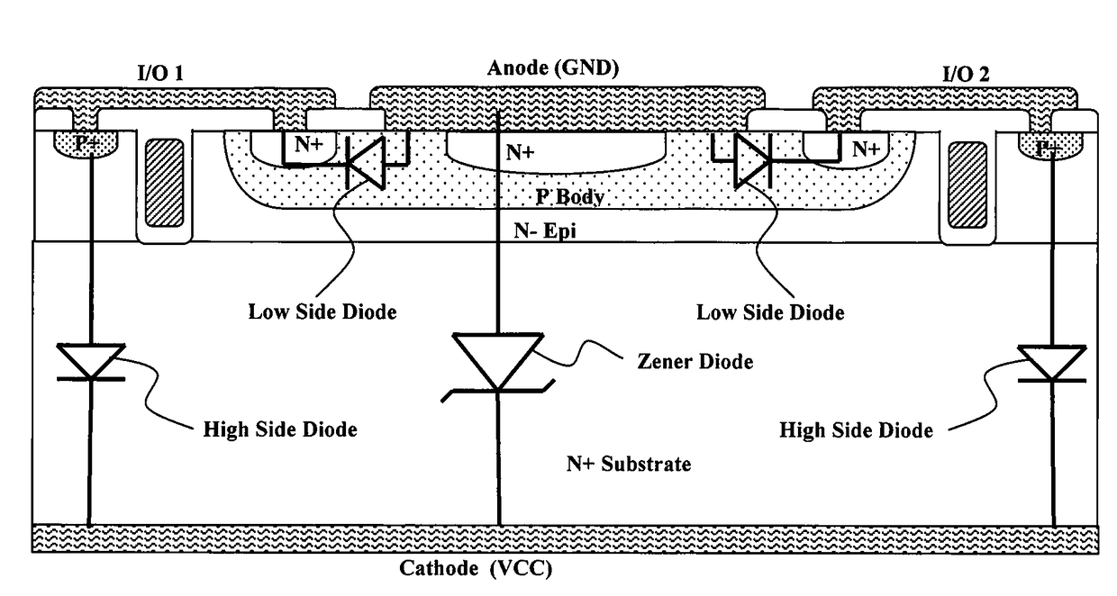
[0012]It is therefore an aspect of the present invention to provide an improved TVS structural configurations implemented with high-side diode, low-side diode functioning as steering diodes. The steering diodes are integrated with a main Zener diode wherein the high-side diode, the low-side diode and the main Zener diode are all manufactured as vertical diodes in a semiconductor substrate. The high-side diode now overlaps with the main Zener diode such that the TVS now occupies significantly less area to allow for further miniaturization of the electronic devices protected by the improved TVS of this invention. The low-cost TVS circuits disclosed in this invention can achieve TVS protections with small silicon die footprint to overcome and resolve the above discussed limitations and difficulties as encountered by the conventional device configuration and manufacturing methods for producing TVS devices.

Problems solved by technology

However, in situations such as electrostatic discharge (ESD), electrical fast transients and lightning, an unexpected and an uncontrollable high voltage may accidentally strike onto the circuit.
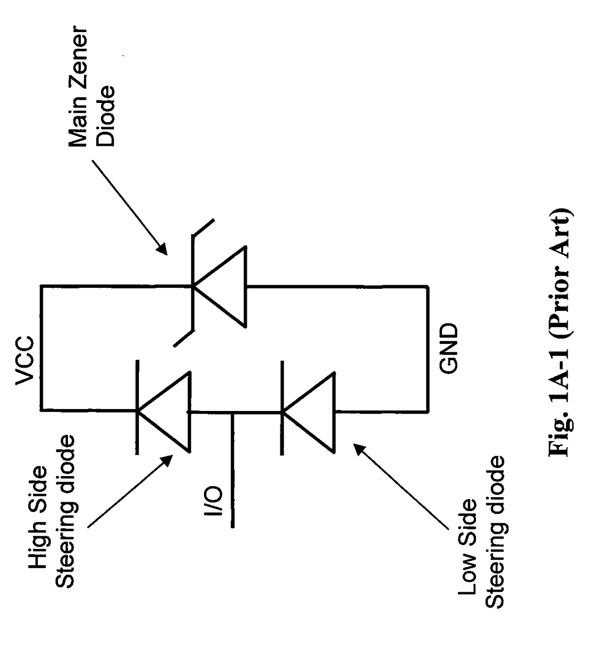
It is therefore difficult to miniaturize the electronic device protected by TVS circuits as shown in FIG. 1B-1.

Method used


Image

  • Optimized configurations to integrate steering diodes in low capacitance transient voltage suppressor (TVS)
  • Optimized configurations to integrate steering diodes in low capacitance transient voltage suppressor (TVS)
  • Optimized configurations to integrate steering diodes in low capacitance transient voltage suppressor (TVS)

Examples


Embodiment Construction

[0034]Refer to FIG. 2 for a side cross sectional view illustrated with equivalent circuit of a transient voltage suppressor (TVS) 100 of this invention. The TVS 100 is formed on a heavily doped P+ semiconductor substrate 105 which supports a P two-layer epitaxial layer 110 that includes a bottom P-epitaxial 110-1 and a top P-epitaxial layer 110-2 with a backside metal 101 disposed below the bottom surface to function as a ground terminal. The TVS 100 includes a P+ region high-side steering diode and Zener diode overlapping zone with a deep voltage breakdown (VBD) trigger implant layer 115 implanted with P+ dopant ions disposed between the bottom epitaxial layer 110-1 and a N+ buried layer 120 disposed below a top N+ source region 125. The Zener diode is formed from the buried layer 120 to the bottom epitaxial layer 110-1. A shallow P+ implant region 130 is formed near the top surface of the top P-epitaxial layer 110-2 to enhance the electrical contact with an I / O metal pad 135. An o...


PUM


Abstract

A transient-voltage suppressing (TVS) device disposed on a semiconductor substrate including a low-side steering diode, a high-side steering diode integrated with a main Zener diode for suppressing a transient voltage. The low-side steering diode and the high-side steering diode integrated with the Zener diode are disposed in the semiconductor substrate and each constituting a vertical PN junction as vertical diodes in the semiconductor substrate whereby reducing a lateral area occupied by the TVS device. In an exemplary embodiment, the high-side steering diode and the Zener diode are vertically overlapped with each other for further reducing lateral areas occupied by the TVS device.

Description

[0001]This patent application is a Divisional application and claims the Priority date of a co-pending application Ser. No. 13 / 869,869 filed by the same Applicants of this application on Apr. 24, 20013. Application Ser. No. 13 / 869,869 is a Divisional application of another application Ser. No. 12 / 286,817 filed on Oct. 1, 2008 and now issued into U.S. Pat. No. 8,431,958. Application Ser. No. 12 / 286,817 is a Continuation in Part (CIP) application of a another patent application with a Ser. No. 11 / 606,602 filed by a common Inventor of this application on Nov. 20, 2006 and now issued into U.S. Pat. No. 7,880,223. This patent application is also a Continuation in Part (CIP) application of another application with a Ser. No. 11 / 600,696 filed by a common Inventor of this application on Nov. 16, 2006 now issued into U.S. Pat. No. 7,781,826. The Disclosures made in the application Ser. Nos. 11 / 600,696, 11 / 606,602, 12 / 286,817 and 13 / 869,869 are hereby incorporated by reference.BACKGROUND OF ...

Claims


Application Information

Patent Timeline
Patent Type & Authority Applications(United States)
IPC IPC(8): H01L27/02H01L21/266H01L29/66H01L29/866H01L29/74
CPCH01L27/0248H01L29/866H01L21/266H01L29/66106H01L29/66371H01L29/7412H01L27/0255H01L29/0649
Inventor BOBDE, MADHUR
Owner ALPHA & OMEGA SEMICON INC
Learn More