Pattern treatment methods

a pattern and treatment method technology, applied in the field of pattern treatment methods, can solve the problems of inability to accurately detect patterns, add to the complexity of the process, and disadvantage in the process throughput, and achieve the effect of high resolution patterns

Inactive Publication Date: 2017-06-15
DOW GLOBAL TECH LLC +1
View PDF7 Cites 13 Cited by
  • Summary
  • Abstract
  • Description
  • Claims
  • Application Information

AI Technical Summary

Benefits of technology

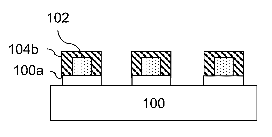
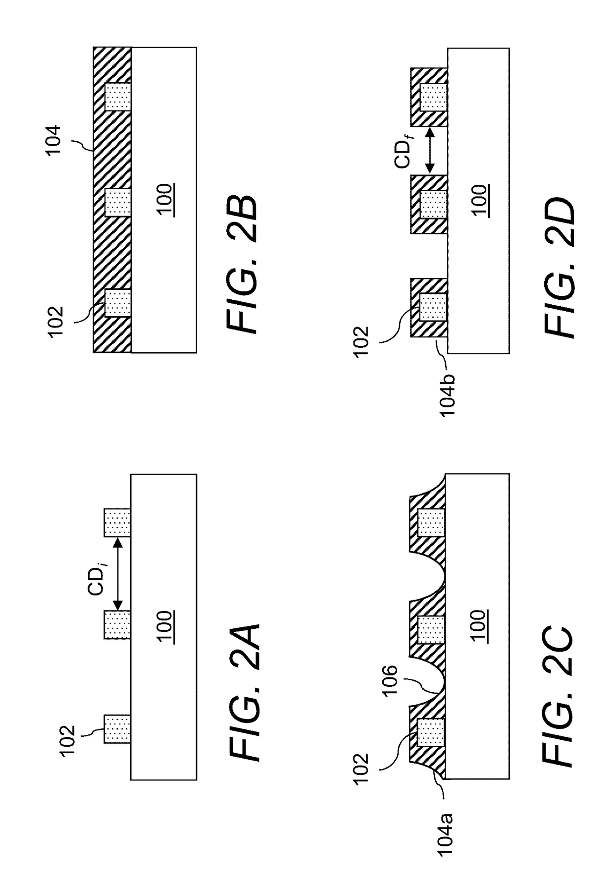
[0008]In accordance with a first aspect of the invention, pattern treatment methods are provided. The methods comprise: (a) providing a semiconductor substrate comprising a patterned feature on a surface thereof; (b) applying a pattern treatment composition to the patterned feature, wherein the pattern treatment composition comprises a polymer comprising a surface attachment group for forming a bond with a surface of the patterned feature and a solvent, and wherein the pattern treatment composition is free of crosslinkers; (c) removing residual pattern treatment composition from the substrate with a first rinse agent, leaving a coating of the polymer over and bonded to the surface of the patterned feature; and (d) rinsing the polymer-coated patterned feature with a second rinse agent that is different from the first rinse agent, wherein the polymer has a solubility that is greater in the first rinse agent than in the second rinse agent. The invention finds particular applicability in the manufacture of semiconductor devices for providing high resolution patterns.

Problems solved by technology

The CVD assist shrink technique requires use of CVD and etching tools which are costly, add to the complexity of the process and are disadvantageous in terms of process throughput.
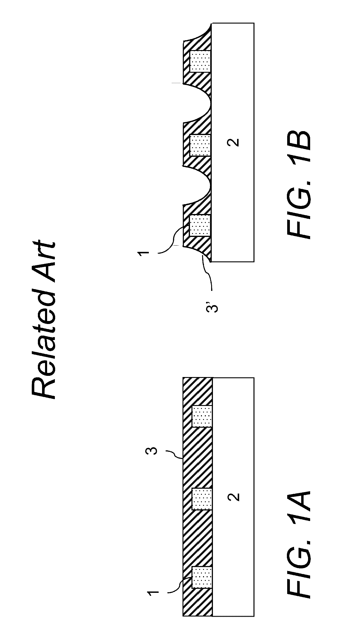
This process typically suffers from iso-dense bias (IDB), wherein growth of the crosslinked layer on the resist pattern occurs non-uniformly across the die surface depending on density (spacing between) adjacent resist patterns.
This can lead to patterning defects and variations in electrical characteristics across the die for what are intended to be identical devices.
Polymer blend self-assembly has been found to suffer from proximity and size effects.
This can lead to the same problems described with respect to the acid diffusion resist growth technique.
The occurrence of footing is undesirable in that it can result in patterning defects, for example, bridging defects or missing contact holes, which can adversely impact device yield.

Method used


Image

  • Pattern treatment methods
  • Pattern treatment methods
  • Pattern treatment methods

Examples


examples

[0068]Number and weight-average molecular weights, Mn and Mw, and polydispersity (PDI) values (Mw / Mn) for the non-nitrogen-containing block polymers were measured by gel permeation chromatography (GPC) on a Waters alliance system equipped with a refractive index detector. Samples were dissolved in HPCL grade THF at a concentration of approximately 1 mg / mL and injected through four Shodex columns (KF805, KF804, KF803 and KF802). A flow rate of 1 mL / min and temperature of 35° C. were maintained. The columns were calibrated with narrow molecular weight PS standards (EasiCal PS-2 , Polymer Laboratories, Inc.). For the nitrogen-containing block on the final block copolymers, the number average molecular weights Mn were calculated based on reactant feed charges.

[0069]Top-down scanning electron micrographs were generated with a Hitachi 59380 SEM at 250 K magnification. Cross-section SEM images were generated with an Amray 1910 scanning electron microscope after sectioning the wafers. Criti...


PUM

PropertyMeasurementUnit
solubilityaaaaaaaaaa
thicknessaaaaaaaaaa
lateral dimensionsaaaaaaaaaa

Abstract

Pattern treatment methods comprise: (a) providing a semiconductor substrate comprising a patterned feature on a surface thereof; (b) applying a pattern treatment composition to the patterned feature, wherein the pattern treatment composition comprises a polymer comprising a surface attachment group for forming a bond with a surface of the patterned feature and a solvent, and wherein the pattern treatment composition is free of crosslinkers; (c) removing residual pattern treatment composition from the substrate with a first rinse agent, leaving a coating of the polymer over and bonded to the surface of the patterned feature; and (d) rinsing the polymer-coated patterned feature with a second rinse agent that is different from the first rinse agent, wherein the polymer has a solubility that is greater in the first rinse agent than in the second rinse agent. The methods find particular applicability in the manufacture of semiconductor devices for providing high resolution patterns.

Description

FIELD OF THE INVENTION[0001]The invention relates generally to the manufacture of electronic devices. More specifically, this invention relates to methods for treating patterns on semiconductor device substrates. The methods find particular use in the manufacture of semiconductor devices in shrink processes for the formation of fine patterns.BACKGROUND OF THE INVENTION[0002]In the semiconductor manufacturing industry, to extend resolution capabilities beyond those obtained with standard resist patterning techniques, various processes for pattern shrink have been proposed. These processes involve increasing the effective thickness of the resist pattern sidewalls to reduce (i.e., “shrink”) the spacing, for example, between adjacent lines or within a trench or hole pattern. In this way, features such as trenches and contact holes formed from the patterns can be made smaller. Known shrink techniques include, for example, chemical vapor deposition (CVD) assist, acid diffusion resist grow...

Claims


Application Information

Patent Timeline
Patent Type & Authority Applications(United States)
IPC IPC(8): H01L21/027C09D125/08G03F7/11C09D133/10H01L21/02G03F7/039
CPCH01L21/0273H01L21/0206C09D125/08G03F7/11C09D133/10G03F7/039G03F7/0035G03F7/004G03F7/09C08F297/02G03F7/0397G03F7/325G03F7/40G03F7/405H01L21/033G03F7/0002G03F7/0025G03F7/16H01L21/02052H01L21/0274
Inventor PARK, JONG KEUNLI, MINGQIKWOK, AMY M.HUSTAD, PHILLIP D.
Owner DOW GLOBAL TECH LLC
Why Eureka
Try Eureka