Circuit structure and manufacturing method thereof

a technology of circuit board and manufacturing method, applied in the manufacture of multi-layer circuits, printed circuit details, electrical connection printed elements, etc., can solve the problem of reducing the layout flexibility of the core layer, and achieve the effect of improving the layout flexibility

Active Publication Date: 2017-06-08
UNIMICRON TECH CORP
View PDF3 Cites 3 Cited by
  • Summary
  • Abstract
  • Description
  • Claims
  • Application Information

AI Technical Summary

Benefits of technology

The invention provides a circuit board structure that allows for better layout flexibility. This is achieved by using a laser resisting layer instead of the inner circuit structure, which allows for larger circuit layout space. After the build-up circuit structures are fabricated, the laser ablation process can be performed to form the cavity that exposes the upper surface of the core layer of the inner circuit structure without affecting the circuit layout of the core layer.

Problems solved by technology

However, since the alignment copper layer is directly formed on the core layer of the inner circuit layer, the circuit layout of the core layer is limited, thus reducing layout flexibility of the core layer.

Method used


Image

  • Circuit structure and manufacturing method thereof
  • Circuit structure and manufacturing method thereof
  • Circuit structure and manufacturing method thereof

Examples


Embodiment Construction

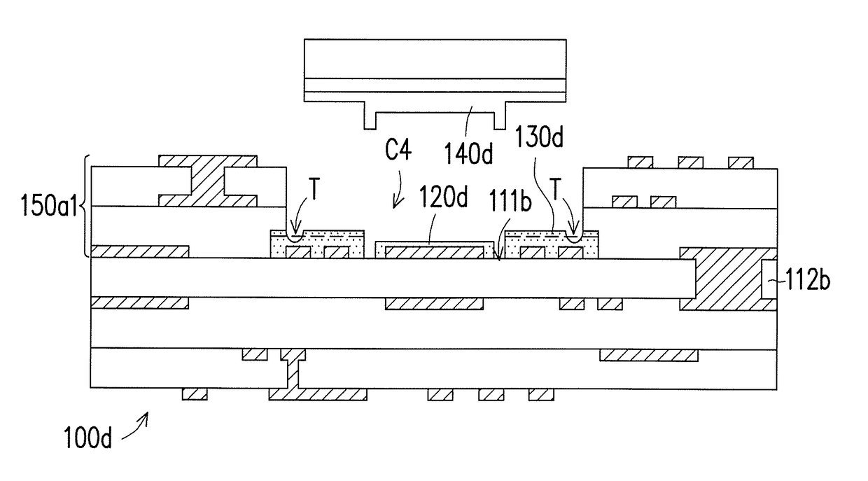
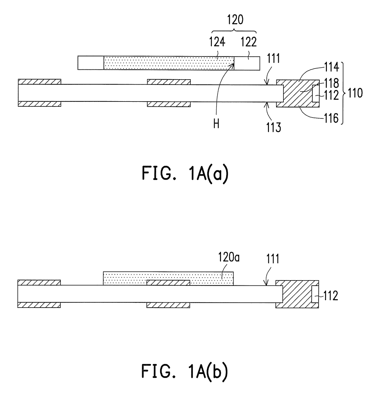
[0034]FIG. 1A(a) to FIG. 1J illustrate cross-sectional schematic views of a manufacturing method of a circuit board structure according to an embodiment of the invention. Referring first to FIG. 1A(a), with regard to the manufacturing method of a circuit board structure according to the present embodiment, first of all, an inner circuit structure 110 is provided, wherein the inner circuit structure 110 includes a core layer 112 having an upper surface 111 and an opposite lower surface 113, a first patterned circuit layer 114 disposed on the upper surface 111 and a second patterned circuit layer 116 disposed on the lower surface 113. As shown in FIG. 1A(a), the first patterned circuit layer 114 and the second patterned circuit layer 116 are electrically connected through at least one conductive through hole 118 passing through the core layer 112.

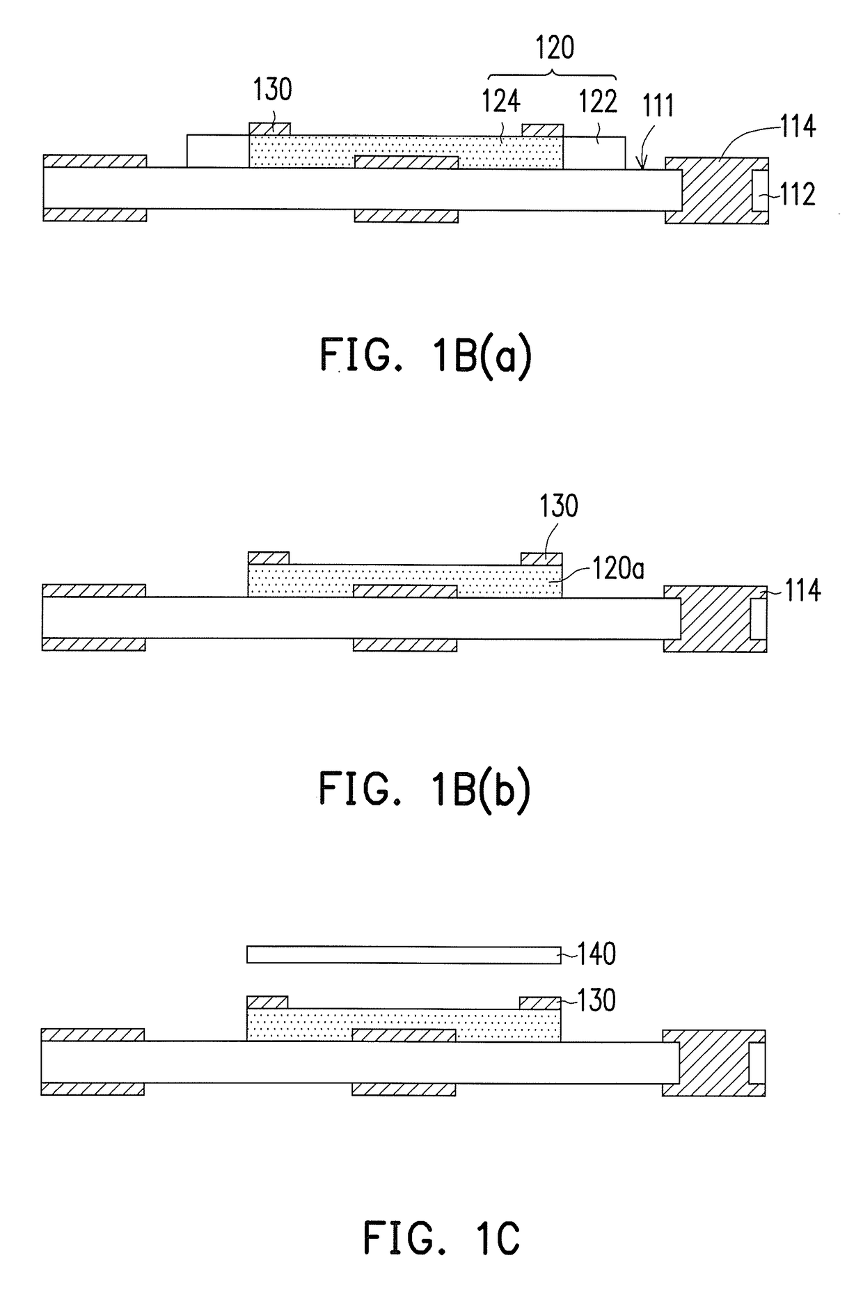
[0035]Next, referring to FIG. 1A(a) and FIG. 1B(a) together, an insulating material layer 120 is formed on a portion of the first patterned ...


PUM


Abstract

A manufacturing method of a circuit board structure is described as follows. An inner circuit structure including a core layer having an upper and an opposite lower surface, a first patterned circuit layer disposed on the upper surface and a second patterned circuit layer disposed on the lower surface is provided. An insulating material layer is formed on a portion of the first patterned circuit layer. A laser resisting layer is formed on at least a portion of the insulating material layer. A release layer is adhered to the laser resisting layer. A build-up process is performed so as to laminate a first and a second build-up circuit structures on the first and the second patterned circuit layers, respectively. A laser ablation process is performed on the first build-up circuit structure so as to form a cavity at least exposing a portion of the upper surface of the core layer.

Description

CROSS-REFERENCE TO RELATED APPLICATION[0001]This application claims the priority benefit of Taiwan application serial no. 104140604, filed on Dec. 3, 2015. The entirety of the above-mentioned patent application is hereby incorporated by reference herein and made a part of this specification.BACKGROUND OF THE INVENTION[0002]Field of the Invention[0003]The invention relates to a circuit board structure and a manufacturing method thereof. More particularly, the invention relates to a circuit board structure having a cavity and a manufacturing method thereof.[0004]Description of Related Art[0005]Generally, to manufacture a circuit board structure having a cavity, it is necessary to fabricate an alignment copper layer on a core layer of an inner circuit layer. The purpose thereof is that during a subsequent process of forming the cavity by performing laser ablation on the circuit structure, the alignment copper layer serves not only as a laser resisting layer for preventing excessive abl...

Claims


Application Information

Patent Timeline
Patent Type & Authority Applications(United States)
IPC IPC(8): H05K1/02H05K3/46H05K1/11
CPCH05K1/0296H05K3/4644H05K1/115H05K1/0298
Inventor CHANG, HUNG-LINWU, MING-HAOCHANG, SYUN-SIAOYU, CHENG-POCHANG, CHI-MIN
Owner UNIMICRON TECH CORP
Why Eureka
Try Eureka