
Monitoring devices and processes based on transformation, destruction and conversion of nanostructures

a technology of nanostructures and monitoring devices, applied in special purpose recording/indication devices, material nanotechnology, instruments, etc., can solve the problems of no reports, however, on devices and processes based on destruction of nanostructures

Inactive Publication Date: 2016-12-01
PATEL GORDHANBHAI
View PDF3 Cites 9 Cited by
  • Summary
  • Abstract
  • Description
  • Claims
  • Application Information

AI Technical Summary

Benefits of technology

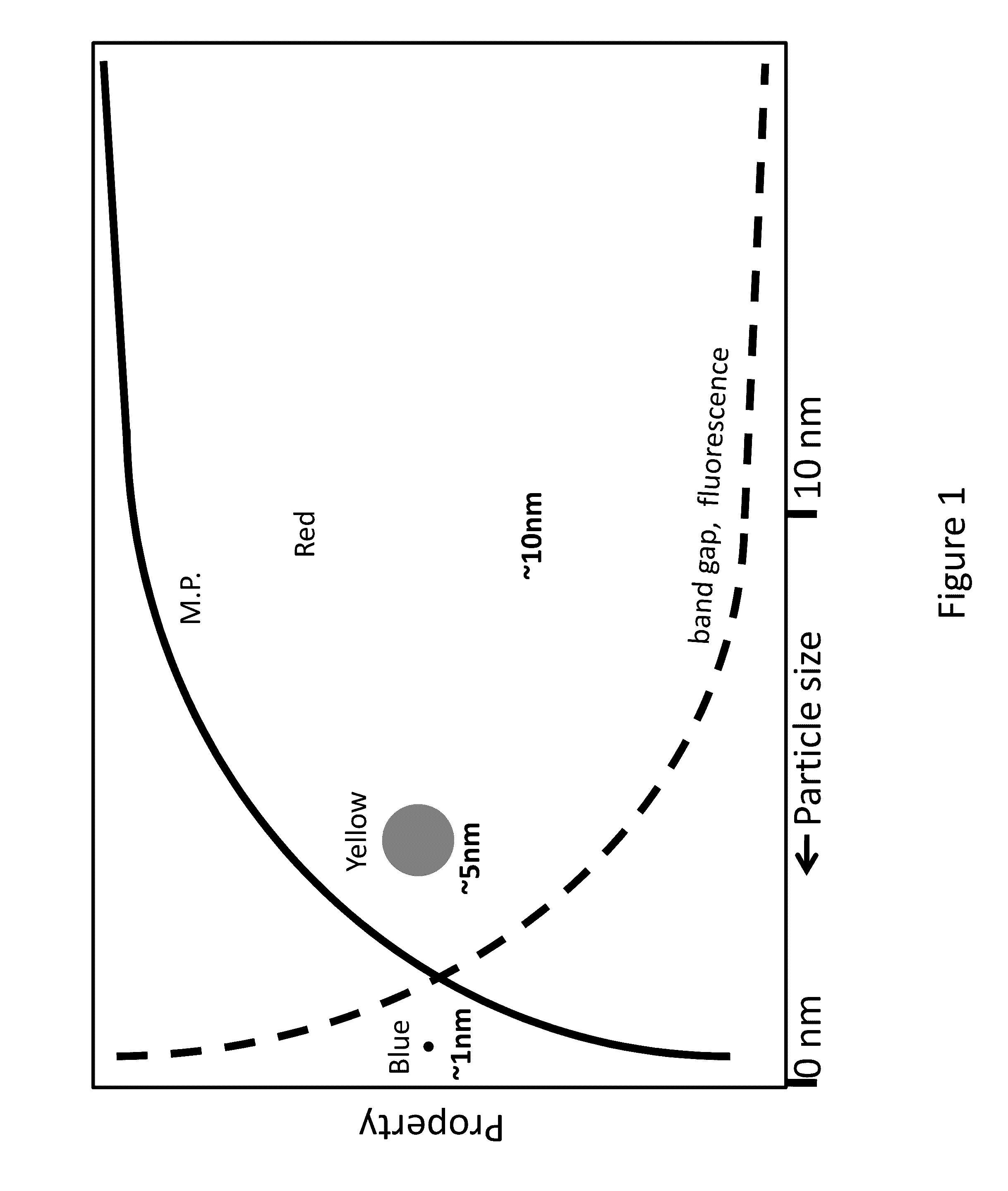
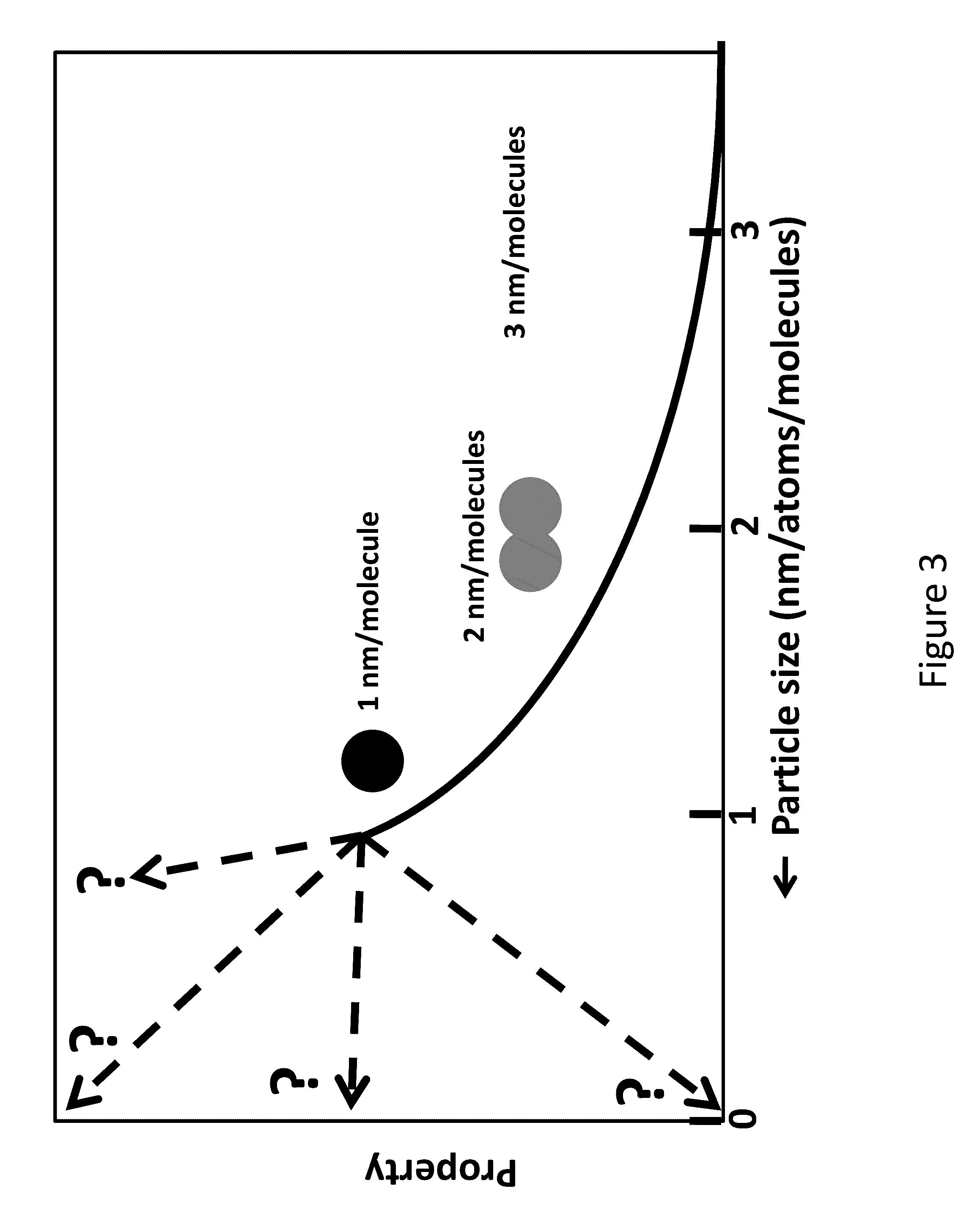
[0011]Thus it is an object of the invention to use this phenomenon to create a variety of devices, products and processes. It is also an object of the present inventions to develop devices, products and processes based on (1) destruction, including reduction in size of nanostructures, (2) higher reactivity of nanostructures, (3) rapid change in properties when size of nanostructures is changed, (4) using unstable nanostructures and alike.
[0017]Another embodiment relates to a process of changing the performance of an indicating nanostructure device which comprises changing a non-linear performance of the indicating device to a linear performance by increasing the size distribution of the nanostructures in the indicating system.
[0053]Still another object is to provide a partially demetallized semiconductive metal susceptor for microwave indicator wherein the heat produced in different areas can be precisely controlled and the various areas producing different amounts of heat can be given any desired shape.

Problems solved by technology

Nanostructures are intrinsically less stable than their counter microstructures.
There are no reports, however, on devices and processes based on destruction of nanostructures.

Method used


Image

  • Monitoring devices and processes based on transformation, destruction and conversion of nanostructures
  • Monitoring devices and processes based on transformation, destruction and conversion of nanostructures
  • Monitoring devices and processes based on transformation, destruction and conversion of nanostructures

Examples


example 1

Making of Capacitor by Coating Halocompounds

[0212]A metallized plastic film (about 3 nm thick layer of aluminum on 2 mil polyester film) was coated with solution of 15 g polyvinyl acetate in 25 g of ethyltrichloroacetate. The coating was laminated with another piece of metallized polyester film. The capacitance of the sandwich was 16.4 micro Faraday. The capacitor was radiated with 400 rads of 100 KeV X-ray. The capacitance changed to 6.1 nano faraday and after about 2 hours the metallized films became clear.

example 2

Change in Electrical Resistance with Ionizing Radiation

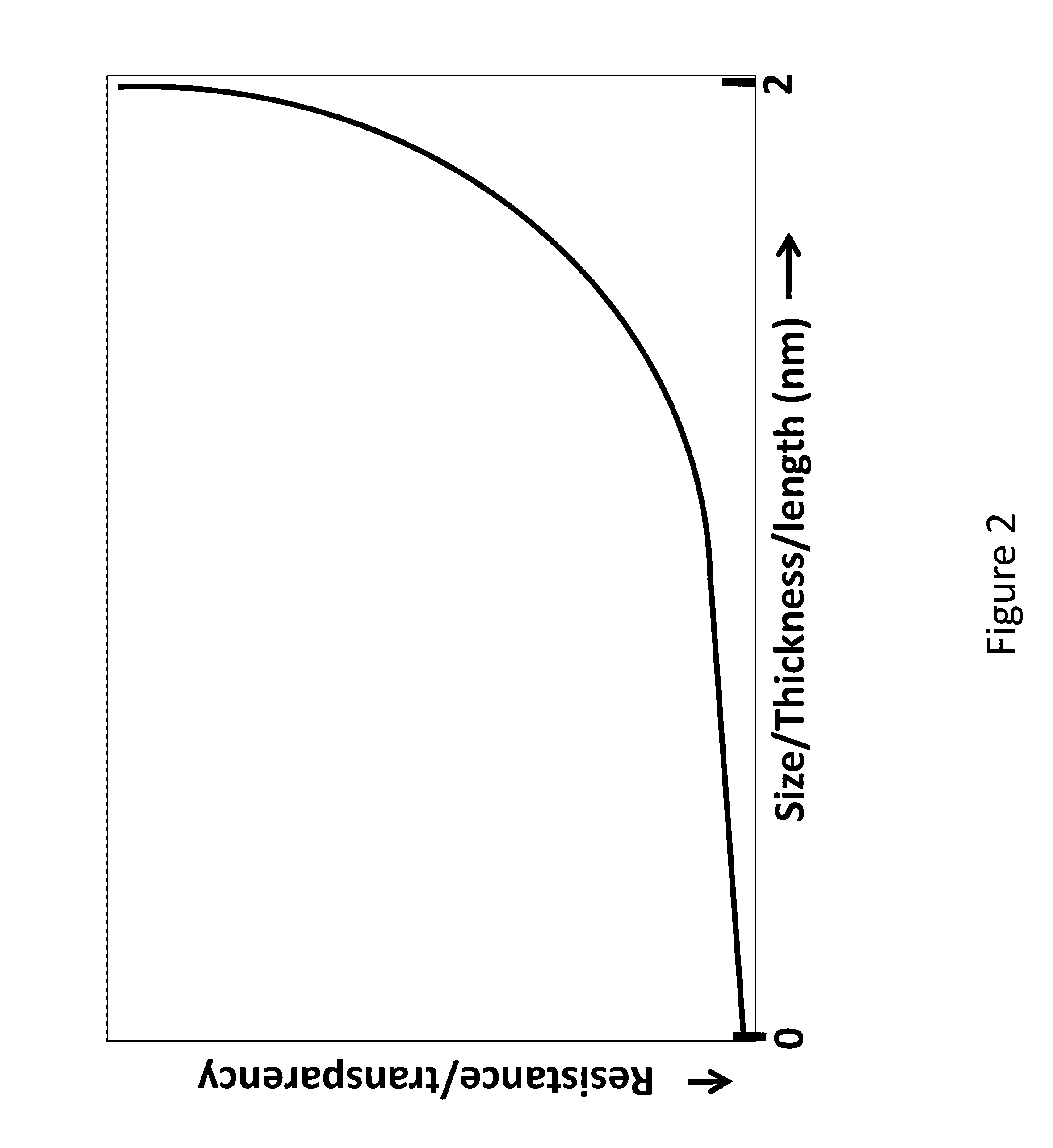
[0213]A metallized plastic film (about 10 nm thick layer of aluminum on 4 mil polyester film) was coated with solution of 15 g polyvinyl acetate in 25 g of ethyltrichloroacetate using #3 gap bar. The coating was laminated with cellophane film. The assembly was connected to an electrometer / multimeter. The film was irradiated to 254 nm 4 watt UV lamp for a minutes at 5 cm distance as shown in FIG. 25(a). The change in electrical resistance was recorded with a video camera. The resistance changed from 0.56 kilo Ohms to 21.6 mega Ohms within a few hours and the film became almost clear (see FIG. 25(b)).

example 3

Change in Electrical Resistance of TTI Device

[0214]A TTI (time-temperature indicator) device was made as per Example 6 of our U.S. patent application Ser. No. 12 / 478,232. The change in electrical resistance was recorded with a video camera at room temperature. The resistance changed from 4.2 Ohms to 18.4 mega Ohms after about 18 hours and the film became almost clear.


PUM

PropertyMeasurementUnit
size distributionaaaaaaaaaa
thicknessaaaaaaaaaa

Abstract

A large number of properties of nanostructures depend on their size, shape and many other parameters. As the size of a nanostructure decreases, there is a rapid change in many properties. When the nanostructure is completely destroyed, those properties essentially disappear. Systems based on changes in properties of nanostructures due to the destruction of nanostructures are proposed. The systems can be used for monitoring the total exposure to organic, inorganic, organometallic and biological compounds and agents using analytical methods.

Description

CROSS-REFERENCES TO RELATED APPLICATIONS[0001]This application is a CIP of U.S. patent application Ser. No. 12 / 478,232 and US provisional patent applications cited therein, incorporated herein by reference in their entireties.[0002]This application claims priority to U.S. Provisional Patent Applications No. 61 / 132,799, filed Dec. 15, 2008; 61 / 162,539, filed Mar. 23, 2009; 61 / 215,982 filed May 12, 2009; and 61 / 276,349 filed Sep. 11, 2009.FIELD OF INVENTION[0003]This invention relates to devices and associated processes based on physical, chemical and biological destruction of nanostructures. This invention also relates to monitoring the total exposure to organic, inorganic, organometallic and biological compounds and agents using unstable, reactive or destructible nanostructures using analytical methods.BACKGROUND OF THE INVENTION[0004]U.S. patent application Ser. No. 12 / 478,232 discloses certain formulations and devices based on the etching of a thin (e.g., 10-100 nm) layer of a met...

Claims


Application Information

Patent Timeline
Patent Type & Authority Applications(United States)
IPC IPC(8): G01D7/00
CPCG01D7/00G01D3/10G01D7/005B82Y15/00B82Y30/00
Inventor PATEL, GORDHANBHAI
Owner PATEL GORDHANBHAI
Learn More