
A connection pin, a converter assembly and a method for manufacturing a connection pin

a technology of connection pin and converter assembly, which is applied in the manufacture of fixed connections, cable/conductor components, printed circuit aspects, etc., can solve the problems of screen printed solder having the drawback of taking up additional space on the pcb that could otherwise be used for circuitry and components, and achieves less defective products, more reliable production process, and high component density.

Inactive Publication Date: 2016-09-22
TELEFON AB LM ERICSSON (PUBL)
View PDF12 Cites 7 Cited by
  • Summary
  • Abstract
  • Description
  • Claims
  • Application Information

AI Technical Summary

Benefits of technology

This patent is about a new type of connection pin that can be used to mount components on computer circuit boards. The pin has a cavity filled with solder, which means that no extra solder needs to be added after the pin is mounted. This simplifies the manufacturing process, reduces the risk of solder bridges, and improves the efficiency of production. The connection pin also allows for higher component density on the circuit board, which means more components can be included in a smaller space, resulting in cost savings.

Problems solved by technology

In the field of power modules, e.g. converters such as dc / dc converters, a major issue is how to increase the number of components per square mm combined with a demand for higher currents and a resulting need for more effective cooling.
The screen printed solder has the drawback of taking up additional space on the PCB that could otherwise be used for circuitry and components.
However, since the required amount of solder paste for each pin sometimes is more than required for the SMT components, there is a need to dispense additional solder paste on the PCB.
The preform will take up space around the hole and reduce the space available for circuitry and components.
All of the proposed alternatives for adding additional solder paste have the drawback of requiring additional steps in the manufacturing process.
On the other hand, if too much solder paste is added, it may overflow onto the PCB during the reflow process and cause solder bridging that will jeopardize the product functionality.
Thus this is a complicated and sensitive part of the manufacturing process that involves risks of low yield and high costs if not adjusted successfully.
Further, the addition of more solder that is required for soldering of the pins, has in most cases the disadvantage of reducing the surface space that is available for circuitry and components on the PCB, and thus reduce component density.

Method used


Image

  • A connection pin, a converter assembly and a method for manufacturing a connection pin
  • A connection pin, a converter assembly and a method for manufacturing a connection pin
  • A connection pin, a converter assembly and a method for manufacturing a connection pin

Examples


Embodiment Construction

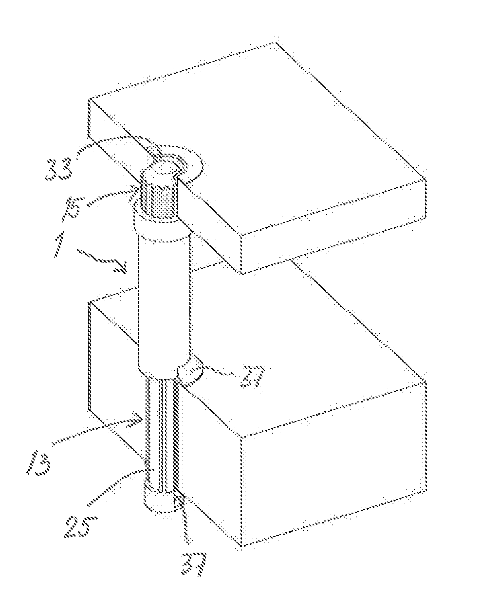
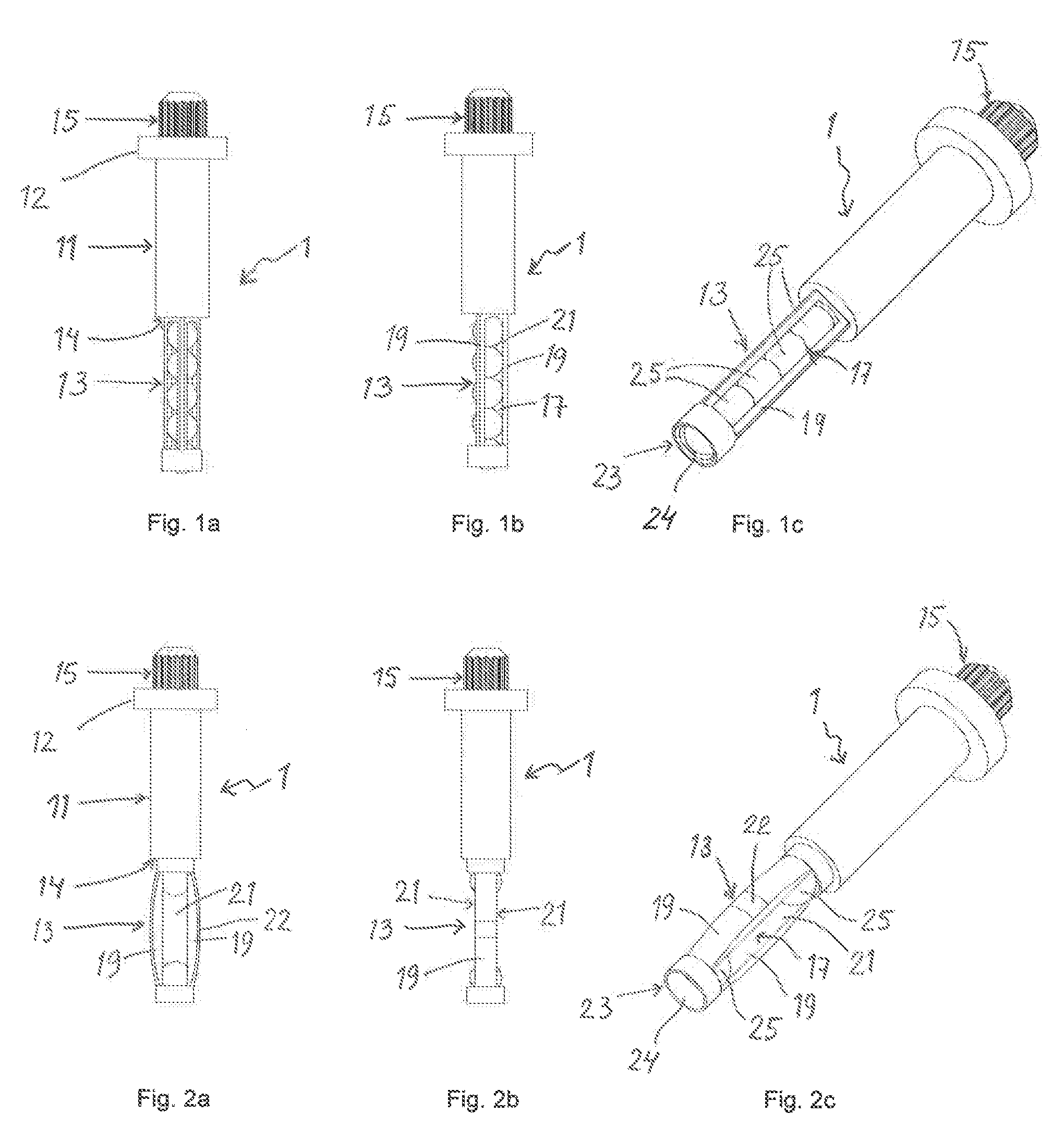
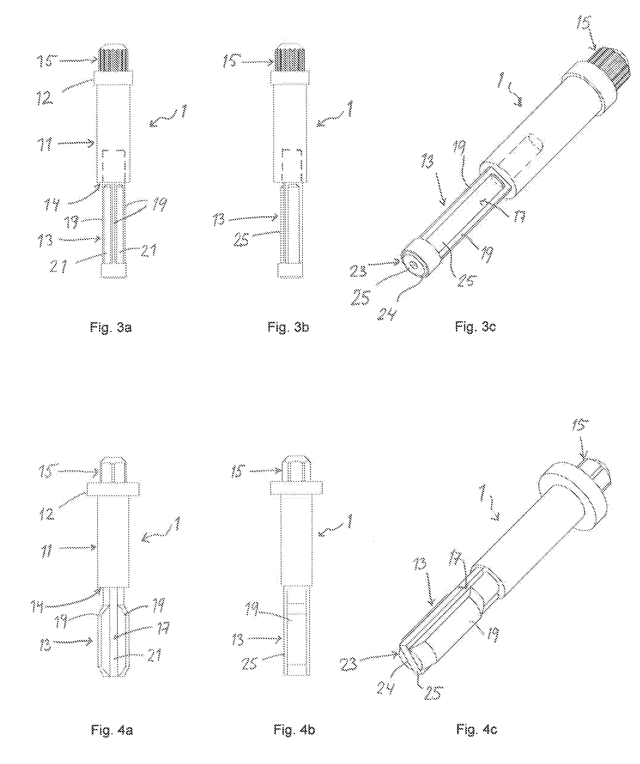
[0045]FIGS. 1a to 1c illustrate a first embodiment of a connection pin 1 according to the present disclosure. The connection pin is made of an electrically and thermally conductive material, e.g. a metal such as copper or brass alloy, and has a general cylindrical shape. The connection pin has a first contact part 13 that is adapted for mounting in a hole in a first PCB. The connection pin has a second contact part 15 that is adapted for mounting in another element, e.g. another, second, PCB. The first contact part 13 comprises an internal cavity 17 surrounded by a wall 19. The wall is provided with at least one wall opening 21, which in the first embodiment is three rectangular openings. The connection pin 1 further has an open end 23 located at the end of the connection pin that is closest to the first contact part 13, and an opening 24 provided by the open end 23 communicates with the cavity 17. Inside the cavity, there is arranged one or several solder preforms 25, which in the ...


PUM


Abstract

A connection pin comprising a first contact part that is adapted for mounting in a hole in a printed circuit board (PCB), and a second contact part. The first contact part comprises a cavity surrounded by a wall, and the wall has at least one opening. At least one solder preform is located in the cavity. A converter assembly comprising a first PCB, and having at least one hole in which a connection pin is mounted. The first PCB with the connection pin is then mounted on a second PCB. Further is described a method for manufacturing a connection pin comprising: providing a connection pin with a cavity in a contact part of the pin, and providing at least one opening in a wall of the cavity, preparing at least one solder preform, and inserting at least one solder preform into the cavity.

Description

TECHNICAL FIELD OF THE INVENTION[0001]The present disclosure relates to a connection pin, such as a connection pin suitable for mounting in a printed circuit board and in a substrate, e.g. a converter substrate. The present disclosure further relates to a converter assembly, and also to a method for manufacturing a connection pin.BACKGROUND[0002]Within the technical areas where printed circuit boards (PCB) and printed wiring boards (PWB) are used, there is a constant demand for higher component density, i.e. increasing the number of components while at the same time the available surface area is minimal. In the field of power modules, e.g. converters such as dc / dc converters, a major issue is how to increase the number of components per square mm combined with a demand for higher currents and a resulting need for more effective cooling.[0003]According to prior art is known a dc / dc converter that is mounted to a printed circuit board (PCB) with solid pin terminals that extend into th...

Claims


Application Information

Patent Timeline
IPC IPC(8): H05K1/14H01B13/00H01B5/06
CPCH05K1/144H01B13/0036H01B5/06H01R4/024H01R4/028H01R12/52H01R12/58H01R43/0235H01R43/0256H05K3/3478H05K3/368H05K2201/10303H05K2201/10984H05K3/3447
Inventor PEREZ-URIA, IGORDRUGGE, LARS
Owner TELEFON AB LM ERICSSON (PUBL)
Learn More