Imaging device and method of manufacturing the same
a technology of imaging device and manufacturing method, which is applied in the direction of solid-state devices, radiation controlled devices, basic electric elements, etc., can solve the disadvantages of light incident on the photodiode, and achieve the effect of improving the mechanical strength of the region where the electrode pad is arranged and improving the mechanical strength of the region
- Summary
- Abstract
- Description
- Claims
- Application Information
AI Technical Summary
Benefits of technology
Problems solved by technology
Method used
Image
Examples
first embodiment
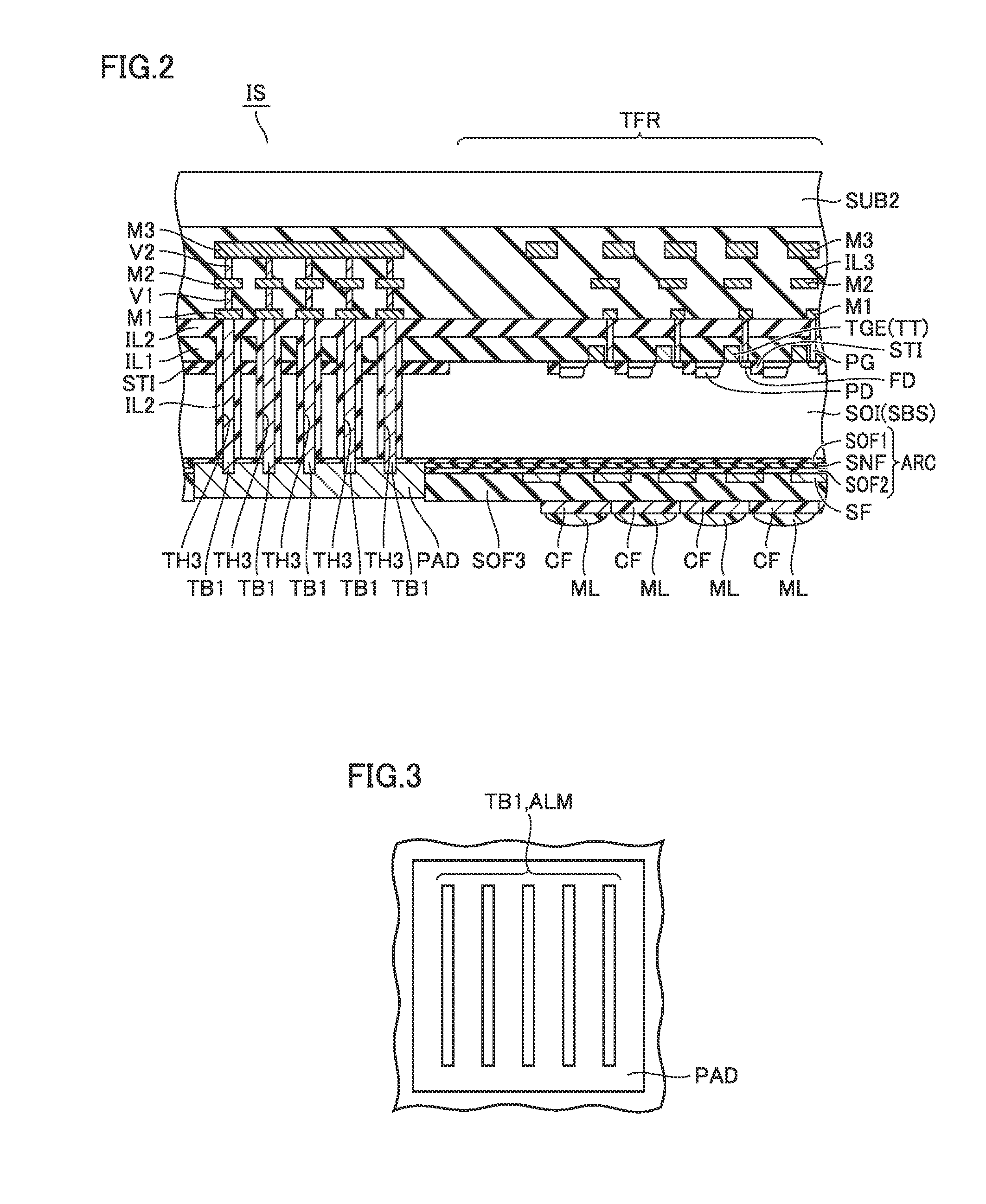
[0070]An imaging device in which an electrode pad and an interconnection are electrically connected to each other by a wall-type conductive pass-through portion will be described here.
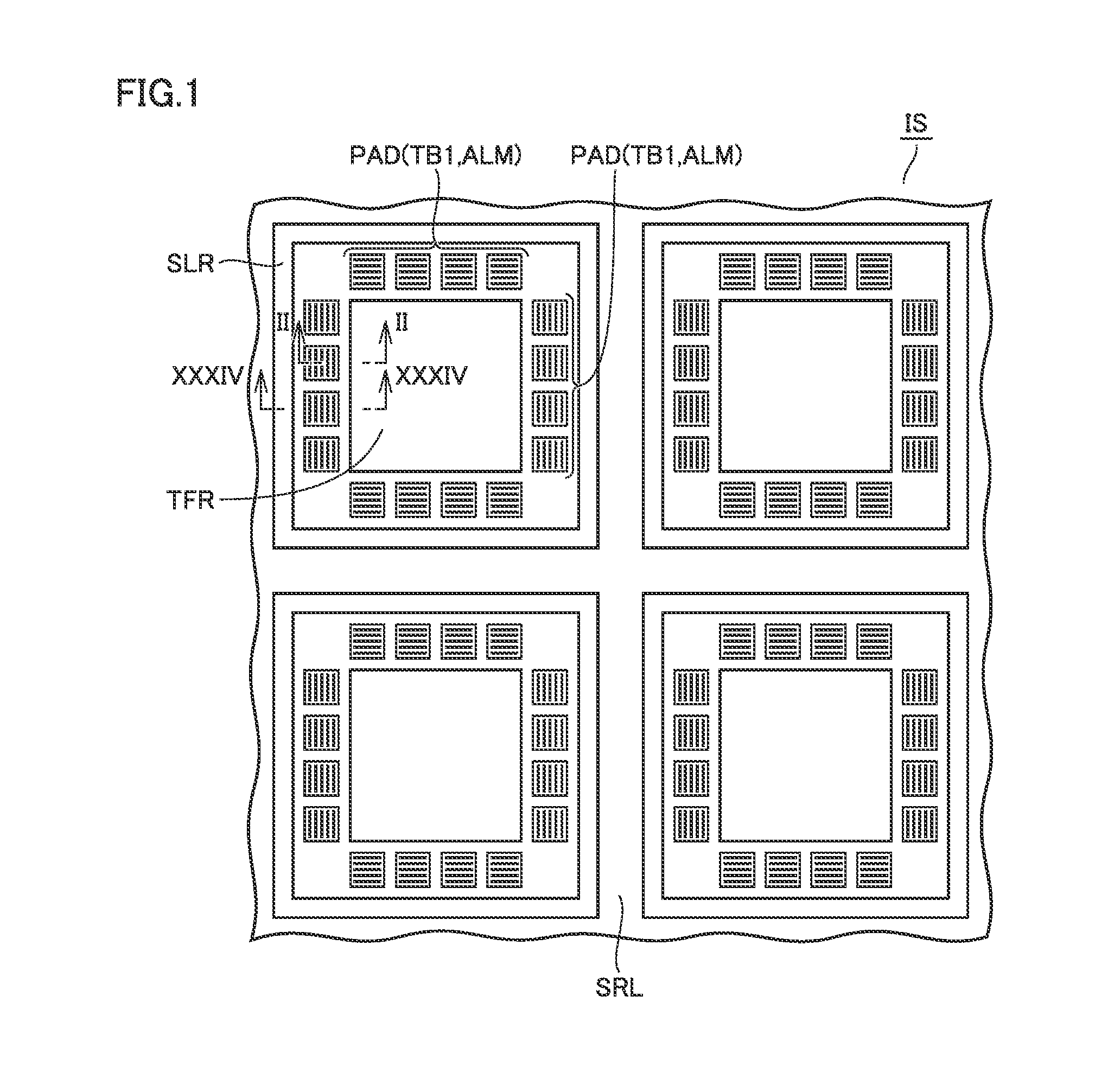
[0071]As shown in FIG. 1, in an imaging device IS, an electrode pad PAD electrically connecting a light reception sensor portion and the outside to each other is arranged around a chip formation region TFR in which the light reception sensor portion including a photodiode is formed. As will be described later, electrode pad PAD is electrically connected to a prescribed interconnection (not shown) by a wall-type conductive pass-through portion TB1 formed in a groove-type through hole passing through a silicon layer. Electrode pad PAD has a function as an alignment mark.
[0072]A seal ring SLR is arranged to surround electrode pads PAD. In a state of a wafer before dicing, a scribe line SRL is located between seal ring SLR and seal ring SLR which are adjacent to each other.
[0073]A structure of electrode pa...
first modification
[0125]In connection with imaging device IS described above, a case that five wall-type conductive pass-through portions TB1 are formed as wall-type conductive pass-through portion TB1 formed in the region where electrode pad PAD is arranged has been described by way of example. The number of wall-type conductive pass-through portions TB1 is not limited to five, but more wall-type conductive pass-through portions TB1 may be formed as shown in FIG. 33.
[0126]Thus, the imaging device according to the first modification can achieve further improved mechanical strength of the region where electrode pad PAD is arranged. Connection resistance between electrode pad PAD and first interconnection M1 (see FIG. 2) can further be lowered.
second modification
[0127]As shown in FIG. 1, in imaging device IS, in order to ensure resistance to moisture, seal ring SLR is formed to surround a region where chip formation region TFR and electrode pad PAD are arranged. A structure of seal ring SLR may be such a structure as being formed simultaneously with the step of forming wall-type conductive pass-through portion TB1 in the region where electrode pad PAD is arranged as shown in FIG. 34.
[0128]Though FIG. 34 has, as reference numerals of portions constituting seal ring SLR, reference numerals the same as those for the portions constituting the region where electrode pad PAD is arranged, those portions do not have corresponding functions.
PUM
 Abstract
Description
Claims
Application Information
 - R&D
- Intellectual Property
- Life Sciences
- Materials
- Tech Scout
- Unparalleled Data Quality
- Higher Quality Content
- 60% Fewer Hallucinations
Browse by: Latest US Patents, China's latest patents, Technical Efficacy Thesaurus, Application Domain, Technology Topic, Popular Technical Reports.
© 2025 PatSnap. All rights reserved.Legal|Privacy policy|Modern Slavery Act Transparency Statement|Sitemap|About US| Contact US: help@patsnap.com


