Optical component and timepiece
a technology applied in the field of optical components and timepieces, can solve the problems of poor productivity of optical components and high production costs, and achieve the effects of excellent appearance, high anti-reflection function, and large influence on the appearance of the entire timepi
- Summary
- Abstract
- Description
- Claims
- Application Information
AI Technical Summary
Benefits of technology
Problems solved by technology
Method used
Image
Examples
first embodiment
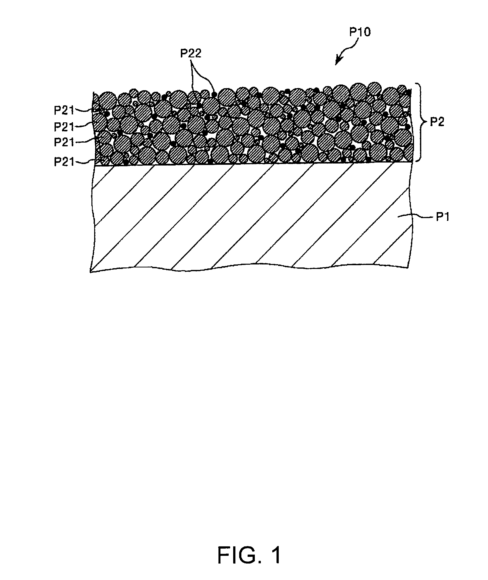
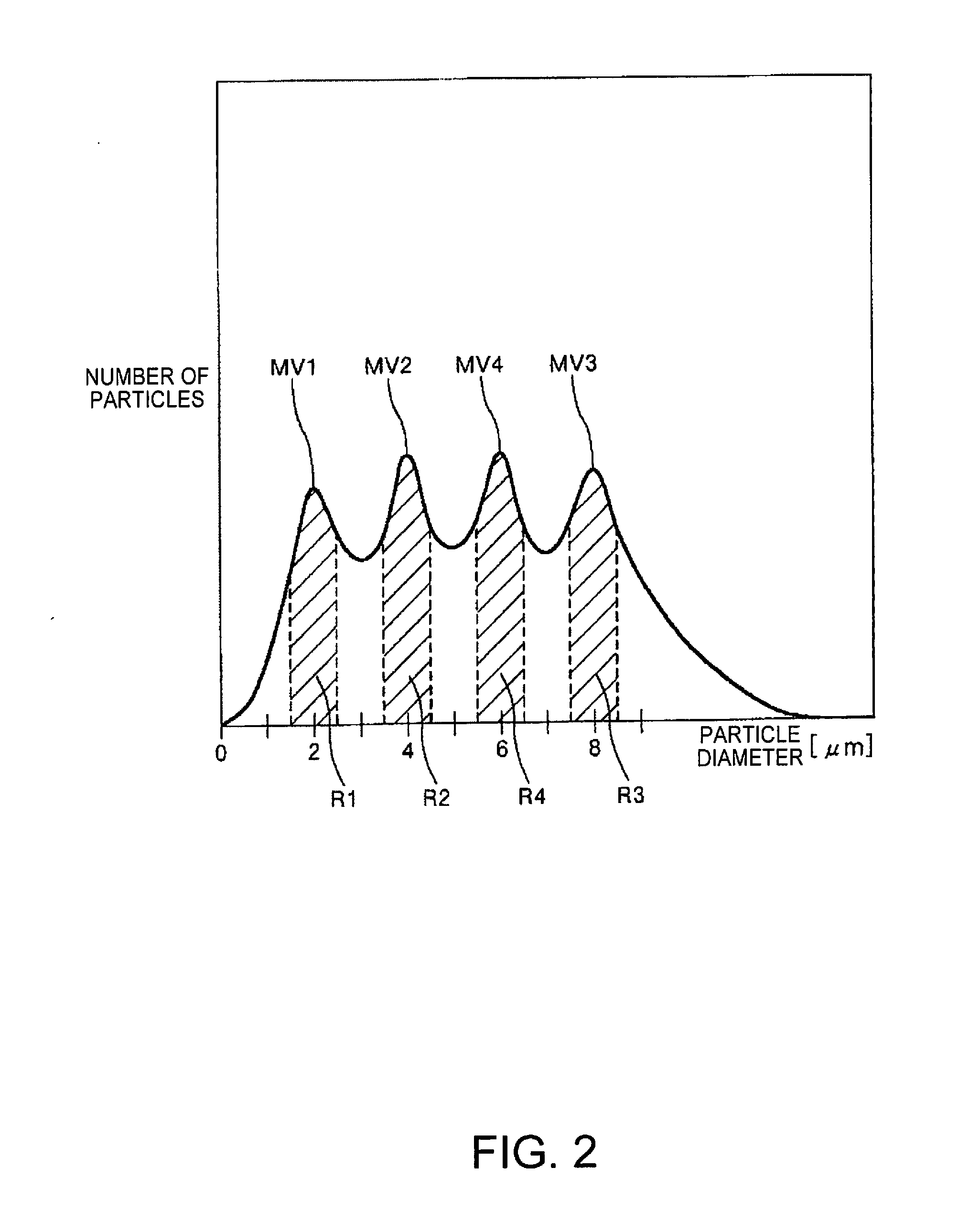
[0036]FIG. 1 is a cross-sectional view schematically showing a first embodiment of an optical component according to the invention, and FIG. 2 is a view schematically showing one example of a particle size distribution of silica particles constituting an antireflection film of an optical component according to the invention.
[0037]As shown in FIG. 1, an optical component P10 of this embodiment includes a base material P1 and an antireflection film P2 containing silica particles P21.
[0038]The silica particles P21 contained in the antireflection film P2 have a given particle size distribution.
[0039]That is, the silica particles P21 contained in the antireflection film P2 have a first local maximum MV1 in the range of 1.5 nm or more and 2.5 nm or less (a first range R1), a second local maximum MV2 in the range of 3.5 nm or more and 4.5 nm or less (a second range R2), and a third local maximum MV3 in the range of 7.5 nm or more and 8.5 nm or less (a third range R3) in a number-based part...
second embodiment
[0112]FIG. 3 is a cross-sectional view schematically showing a second embodiment of the optical component according to the invention. In the following description, different points from the above embodiment will be mainly described, and the description of the same matter will be omitted.
[0113]As shown in FIG. 3, an optical component P10 of this embodiment includes abase material P1, an antireflection film P2 containing silica particles P21, and a foundation layer P3.
[0114]In this manner, by including the foundation layer P3, for example, the adhesiveness between the base material P1 and the antireflection film P2 (the adhesiveness through the foundation layer P3) can be made particularly excellent, and thus, the durability and reliability of the optical component P10 can be made particularly excellent.
[0115]Examples of a constituent material of the foundation layer P3 include various resin materials and SiO2.
[0116]The thickness of the foundation layer P3 is not particularly limited,...
example 1
[0182]By the method as described below, a cover glass as an optical component was produced.
[0183]First, a plate material (glass plate) composed of a sapphire glass was prepared as a base material (the base material preparation step), and a necessary part was cut and polished. The base material obtained by cutting and polishing had a substantially disk shape and had a size of 30 mm in diameter and 1 mm in thickness.
[0184]Subsequently, a UV irradiation treatment in which an ultraviolet ray with a wavelength of 248 nm was irradiated on the surface of the base material on the side where an antireflection film was going to be formed.
[0185]Subsequently, an antireflection film forming composition was applied onto the entire surface of one side of the base material by a spray coating method (antireflection film forming composition application step).
[0186]As the antireflection film forming composition, a composition obtained by mixing silica particles, tin oxide (SnO2) particles (number-base...
PUM
| Property | Measurement | Unit |
|---|---|---|
| number-based particle size distribution | aaaaa | aaaaa |
| number-based particle size distribution | aaaaa | aaaaa |
| number-based particle size distribution | aaaaa | aaaaa |
Abstract
Description
Claims
Application Information
 - R&D
- Intellectual Property
- Life Sciences
- Materials
- Tech Scout
- Unparalleled Data Quality
- Higher Quality Content
- 60% Fewer Hallucinations
Browse by: Latest US Patents, China's latest patents, Technical Efficacy Thesaurus, Application Domain, Technology Topic, Popular Technical Reports.
© 2025 PatSnap. All rights reserved.Legal|Privacy policy|Modern Slavery Act Transparency Statement|Sitemap|About US| Contact US: help@patsnap.com


