
Method of manufacturing printed-circuit board assembly

Active Publication Date: 2016-04-28
SAMSUNG ELECTRONICS CO LTD
View PDF22 Cites 33 Cited by
  • Summary
  • Abstract
  • Description
  • Claims
  • Application Information

AI Technical Summary

Benefits of technology

This patent describes a method for manufacturing a printed circuit board assembly that improves heat dissipation and eliminates manual operations. The method involves filling the space between a package and a shield unit with a heat dissipation material to bond the shield unit and transfer heat away from the package. The method also suggests using a liquid heat-dissipation material that allows for better heat transfer and adhesion force. Additionally, the method eliminates the need for manually fastening a shield unit cover to which the heat dissipation material is applied to decrease compressive stress and make the electronic device slimmer.

Problems solved by technology

While the mechanical shielding type is easy to repair, it requires an additional process for screw fastening and has the weakest reliability, compared to other types of shield unit mounting structures.
The clip type is advantageous in terms of repair, space, and cost, but still requires a manual process for cover fastening and has a lower reliability than the frame type.
However, due to the pick-up space and the width of the frame, the frame type has limitations in an under-fill applying process for a component bonded to the lower side of the frame and in a working space for repairing the component, and has a drawback that the height of the component increases.
However, after a shield unit is mounted, an under-fill resin cannot be applied to an IC component below the shield unit, and thus, the cover type cannot be applied to the mounting portion of a component requiring under-fill.
However, active elements consuming a large amount of power, such as an application processor (AP), a power amplifier module (PAM), a power management integrated circuit (PMIC), etc., generate a great deal of heat while operating.
Such a technology has a limitation in productivity enhancement, however, because the shield unit cover is manually fastened in the process.
This is problematic in terms of product reliability because the compressive stress of the radiant-heat material between the component and the shield unit is transmitted to the whole substrate.

Method used


Image

  • Method of manufacturing printed-circuit board assembly
  • Method of manufacturing printed-circuit board assembly
  • Method of manufacturing printed-circuit board assembly

Examples


Embodiment Construction

[0033]Various embodiments of the present disclosure will now be described in detail with reference to the accompanying drawings. In the following description, specific details such as detailed configurations and components are merely provided to assist the overall understanding of these embodiments of the present disclosure. Therefore, it should be apparent to those skilled in the art that various changes and modifications of the embodiments described herein can be made without departing from the scope and spirit of the present disclosure. In addition, descriptions of well-known functions and constructions are omitted for clarity and conciseness.

[0034]Herein, the terms “include”, “have”, or “may include” indicate the presence of functions, features, numbers, steps, operations, elements, parts, etc., but do not preclude the presence or addition of other functions, features, numbers, steps, operations, elements, parts, etc.

[0035]Herein, the terms “or”, “at least one of”, and “and / or” ...


PUM

PropertyMeasurementUnit
Temperatureaaaaaaaaaa

Abstract

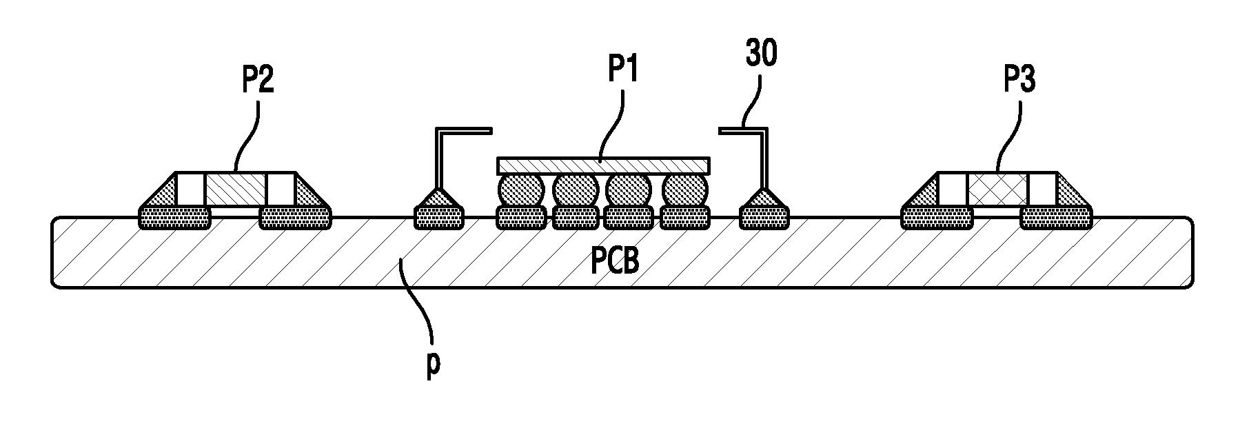
A method is provided for manufacturing a printed circuit board assembly. A method includes applying a liquefied radiant-heat material on a heating component mounted on the printed circuit board; mounting a shield unit on the printed circuit board in contact with the liquefied radiant-heat material; and simultaneously curing the liquefied radiant-heat material and bonding the shield unit.

Description

PRIORITY[0001]This application claims priority under 35 U.S.C. §119(a) to Korean Application Serial No. 10-2014-0144242, which was filed in the Korean Intellectual Property Office on Oct. 23, 2014, the entire disclosure of which is incorporated herein by reference.BACKGROUND[0002]1. Field of the Invention[0003]The present disclosure relates generally to the manufacturing of a printed circuit board assembly, and more particularly, to a method that mounts an electronic component on a printed circuit board of an electronic device.[0004]2. Description of the Related Art[0005]When electronic devices operate, electronic components in the electronic devices emit electromagnetic waves. Since the emitted electromagnetic waves may create noise in the communication functions of the electronic devices, shield parts, i.e., shield unit mounting structures, for blocking the electromagnetic waves are often provided on upper surfaces of the electronic components, when the electronic components are m...

Claims


Application Information

Patent Timeline
IPC IPC(8): H05K3/32H05K3/34
CPCH05K3/341H05K3/321H05K1/0203H05K3/305H01L23/10H01L21/563H01L23/552H01L24/16H01L24/29H01L24/32H01L24/73H01L24/81H01L24/83H01L24/92H05K1/023H05K3/3494H01L2224/16227H01L2224/16238H01L2224/29194H01L2224/32225H01L2224/32245H01L2224/73203H01L2224/73204H01L2224/73253H01L2224/81191H01L2224/81193H01L2224/81815H01L2224/83191H01L2224/83855H01L2224/92125H01L2224/9221H01L2224/92225H01L2924/1421H01L2924/16235H01L2924/16251H01L2924/19105H01L2924/3025H05K2201/066H05K2201/10371H05K2201/1056H01L23/36H01L23/3737H01L23/42H01L23/4275H05K1/0216H01L2224/16225H01L2924/16152Y02P70/50H01L2924/00
Inventor BANG, JUNG-JEKIM, MI-JINLEE, SAE-BOMHAN, HYUN-JOOKIM, KUN-TAK
Owner SAMSUNG ELECTRONICS CO LTD
Learn More