Semiconductor evaluation apparatus and semiconductor evaluation method

Active Publication Date: 2016-04-28
ROHM CO LTD
View PDF3 Cites 0 Cited by
  • Summary
  • Abstract
  • Description
  • Claims
  • Application Information

AI Technical Summary

Benefits of technology

The patent text explains a new technology that allows for better insulation in the evaluation of vertical semiconductor devices. This technology allows for a larger area of high potential, making it easier to secure insulation. Overall, this technology improves the quality and efficiency of semiconductor device evaluations.

Problems solved by technology

The longer cable causes a greater parasitic inductance in a measurement path, resulting in the problem that accuracy of the evaluation of the vertical semiconductor devices deteriorates.
In the conventional technology, however, portions (chuck stage and probe contact region in Japanese Patent Application Laid-Open No. 2013-118320) at high voltage have large areas and they are close to each other, resulting in a problem that securing insulation is more difficult as the voltage applied in an evaluation is increased.

Method used


Image

  • Semiconductor evaluation apparatus and semiconductor evaluation method
  • Semiconductor evaluation apparatus and semiconductor evaluation method
  • Semiconductor evaluation apparatus and semiconductor evaluation method

Examples


first preferred embodiment

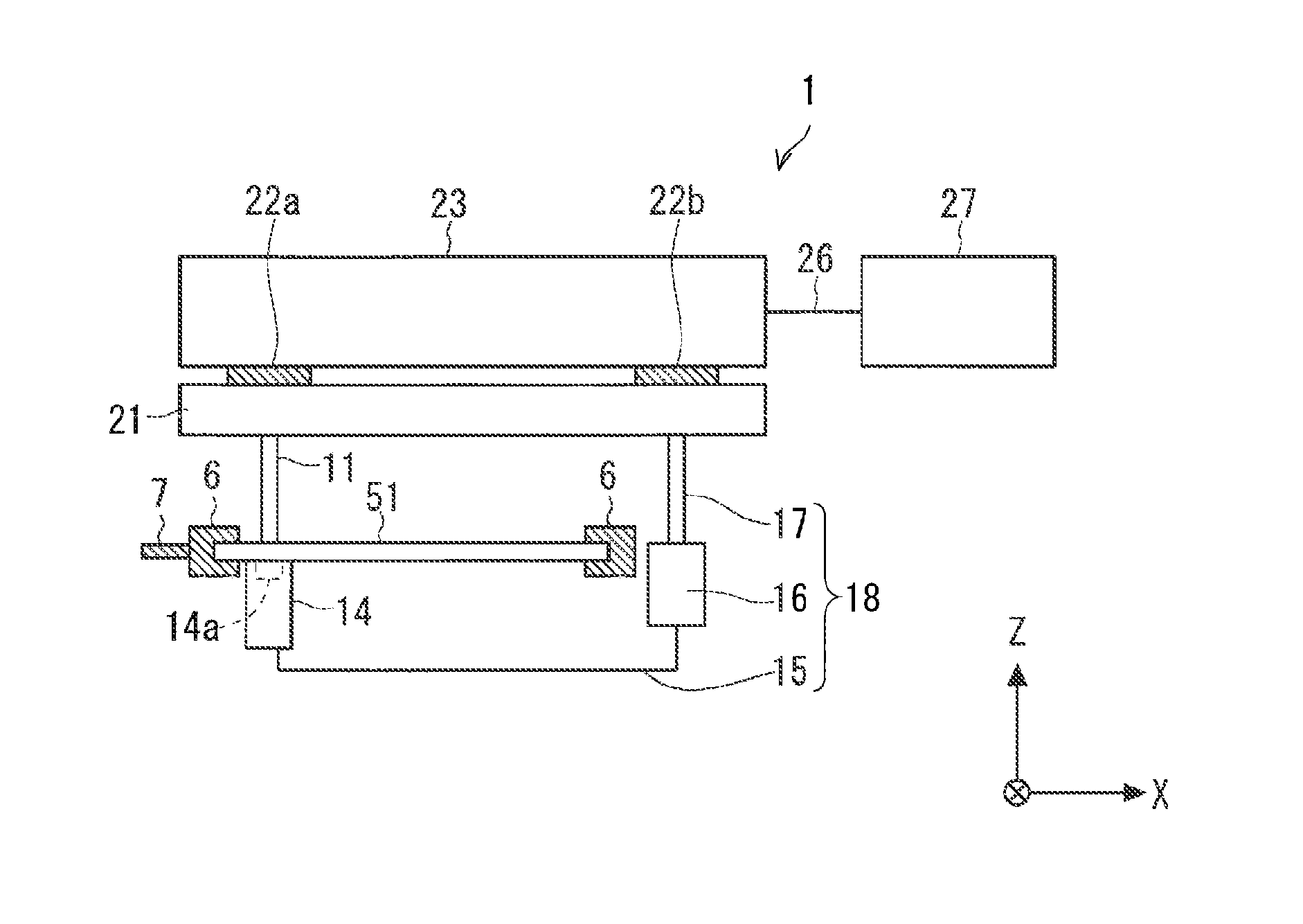
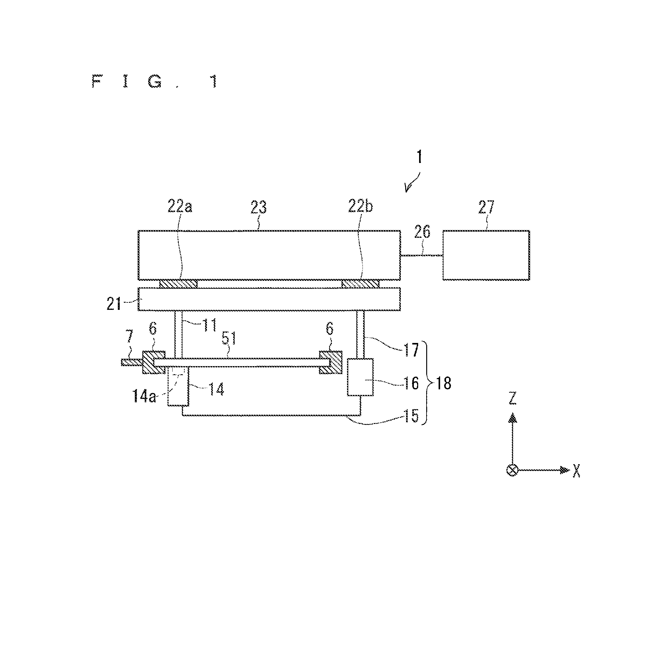
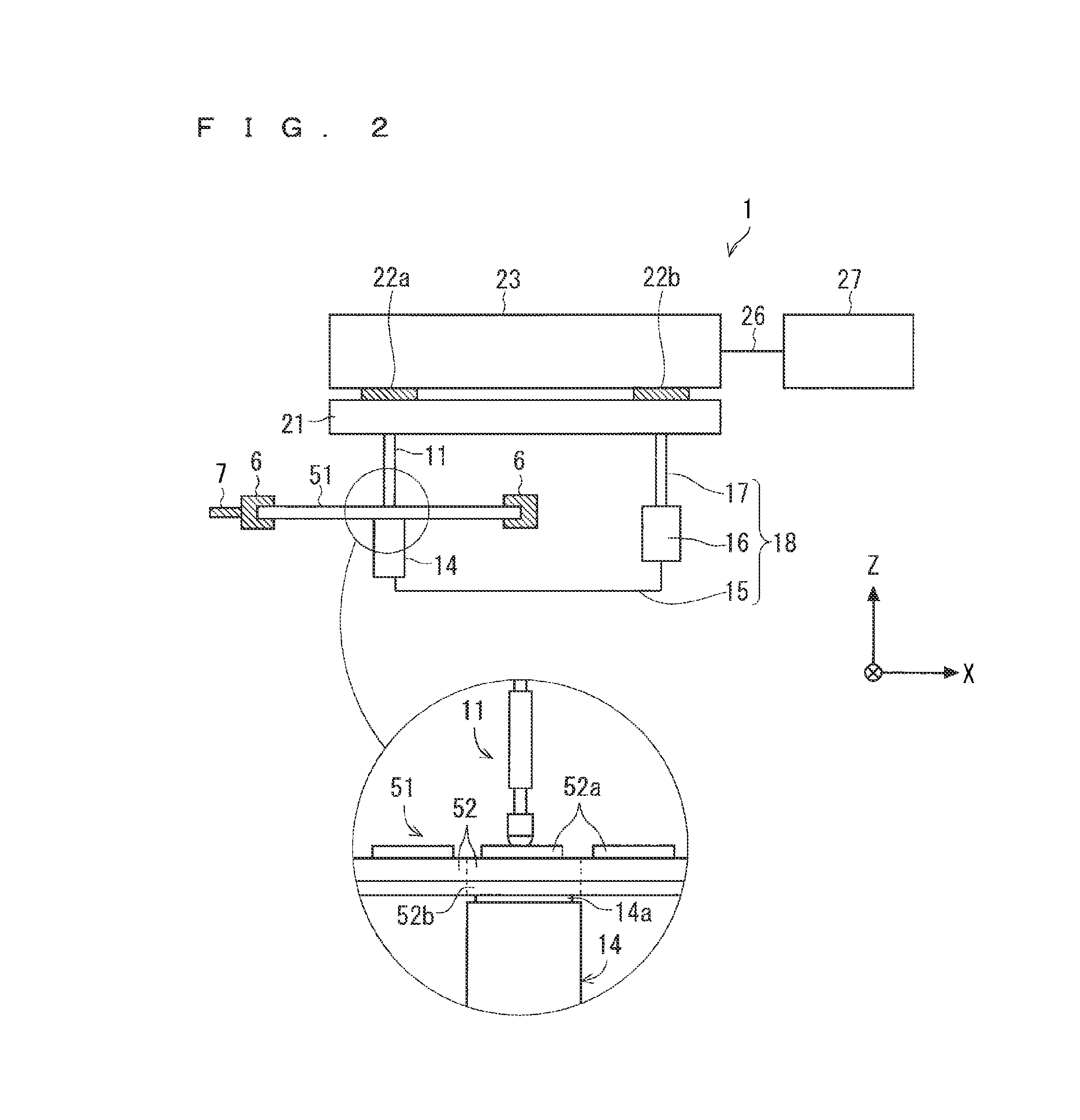
[0023]FIGS. 1 and 2 are cross-sectional views showing a schematic configuration of a semiconductor evaluation apparatus 1 according to a first preferred embodiment of the present invention. FIGS. 1 and 2 show different operation states of the semiconductor evaluation apparatus 1. In addition, FIG. 2 also shows an enlarged view of a portion in a circle.

[0024]The semiconductor evaluation apparatus 1 is a device that evaluates a plurality of vertical semiconductor devices 52 provided in a semiconductor wafer 51, namely, semiconductor devices such as a transistor and a diode having a vertical structure capable of passing a great current in out-of-plane directions (vertical direction, Z direction). As shown in FIG. 2, the vertical semiconductor devices 52 being subjected to the evaluation include front surface electrodes 52a and a back surface electrode 52b provided on a front surface (+Z side) and a back surface (−Z side) of the semiconductor wafer 51, respectively. In addition, the fro...

second preferred embodiment

[0112]FIGS. 13 and 14 are cross-sectional views showing schematic configurations of a semiconductor evaluation apparatus 1 according to a second preferred embodiment of the present invention. FIG. 13 and FIG. 14 show different configurations from each other. In the semiconductor evaluation apparatus 1 according to the second preferred embodiment, the same components as or similar components to those described above are denoted by the same references, and differences will be mainly described.

[0113]In the second preferred embodiment, the extension electrode front surface probe 17 is omitted, and the extension electrode 16 extends to the probe substrate 21 along the Z direction and is electrically connected to the probe connecting portion 22b. In other words, the back surface potential lead-out portion 18 is formed of the wiring portion 15 and the extension electrode 16, and the wiring portion 15 serves as the one end portion of the back surface potential lead-out portion 18 while the ...


PUM


Abstract

A back surface potential lead-out portion has one end portion disposed in a side of a back surface of a semiconductor wafer held by a semiconductor wafer holding portion and the other end portion disposed in a side of a front surface of the semiconductor wafer held by the semiconductor wafer holding portion. The semiconductor wafer and the semiconductor wafer holding portion that holds the semiconductor wafer are movable in an in-plane direction of the semiconductor wafer. In a case where the semiconductor wafer and the semiconductor wafer holding portion that holds the semiconductor wafer are moved in the in-plane direction, a portion of the back surface potential lead-out portion located in the in-plane direction from the semiconductor wafer is fixed close to the outside of a movement region of the semiconductor wafer.

Description

BACKGROUND OF THE INVENTION[0001]1. Field of the Invention[0002]The present invention relates to a semiconductor evaluation apparatus that evaluates a plurality of vertical semiconductor devices provided in a semiconductor wafer and to a semiconductor evaluation method therefor.[0003]2. Description of the Background Art[0004]A method of bringing a mounting surface of an object to be measured into contact with a chuck stage and fixing the mounting surface thereon by vacuum adsorption is commonly used when electrical characteristics of the object to be measured, such as a semiconductor wafer and a semiconductor chip, are measured (evaluated). In an evaluation apparatus that evaluates semiconductor devices having a vertical structure capable of passing current in out-of-plane directions of the semiconductor wafer, the chuck stage that fixes the mounting surface of the semiconductor wafer is used as one of measurement electrodes. In such evaluation apparatus, a cable connected to the ch...

Claims


Application Information

Patent Timeline
IPC IPC(8): G01R1/04G01R1/067
CPCG01R1/06722G01R1/0491
Inventor OKADA, AKIRAHATOZAKI, KOSUKEYAMASHITA, KINYA
Owner ROHM CO LTD
Why Eureka
Try Eureka