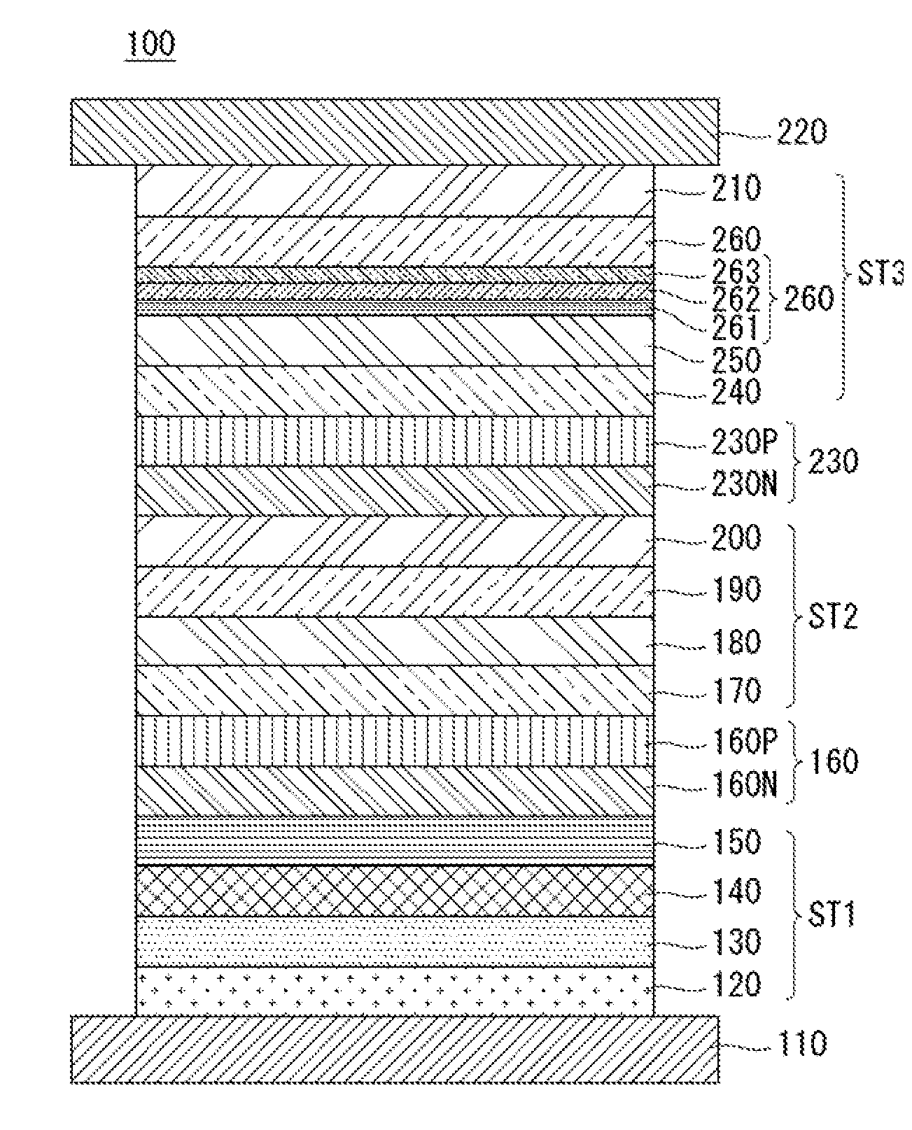
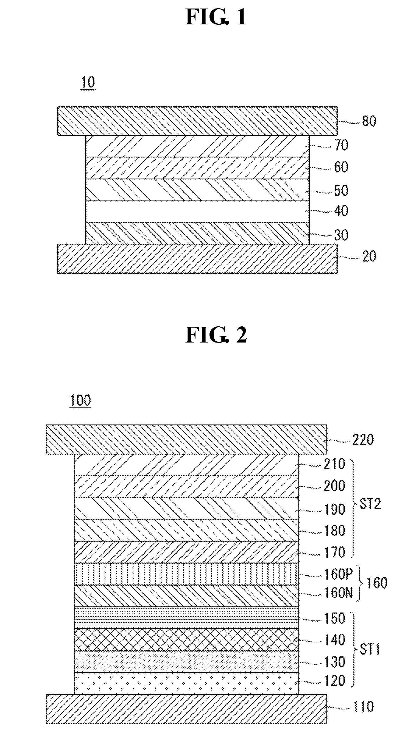
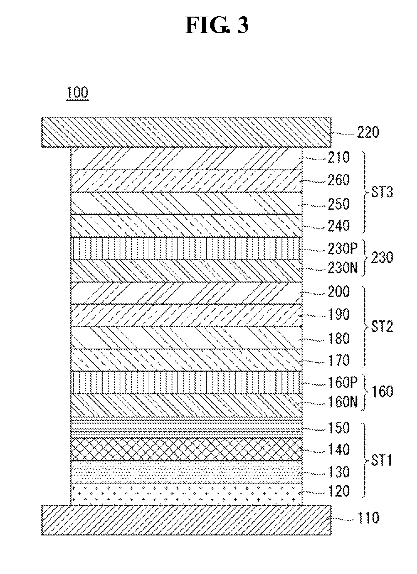
Organic light emitting display device
a light-emitting display and organic technology, applied in the direction of organic semiconductor devices, thermoelectric devices, solid-state devices, etc., can solve the problems of increasing operating voltage, reducing lifetime and efficiency, etc., and achieve the effect of improving emission efficiency and reducing operating voltag
- Summary
- Abstract
- Description
- Claims
- Application Information
AI Technical Summary
Benefits of technology
Problems solved by technology
Method used
Image

Examples
embodiment 1
[0152]An organic light emitting display device having the same composition as Comparative Example 1 was manufactured by using a mixture of an oxadiazole compound and a quinoline compound as the electron transport layer.
[0153]The materials for the electron transport layer used in Comparative Examples 1 and 2 and Embodiment 1 do not limit the scope of the present invention.
[0154]The operating voltage and emission efficiency of the devices manufactured according to Comparative Example 1 and Embodiment 1 were measured and shown in the following Table 1. The operating voltage and emission efficiency of the devices manufactured according to Comparative Example 2 and Embodiment 1 were measured and shown in the following Table 2. In the following Table 1, the measurements taken from Embodiment 1 were expressed as a percentage relative to those taken from Comparative Example 1 corresponding to 100%. In the following Table 2, the measurements taken from Embodiment 1 were expressed as a percen...
embodiment 2
[0157]Devices were manufactured by mixing an oxadiazole compound and a quinoline compound in different ratios: 7:3, 1:1, and 3:7 for an electron transport layer, under the same process condition as Embodiment 1. Here, the ratio may refer to the portion of occupied volume within the electron transport layer.
[0158]The materials for the electron transport layer of Embodiment 2 do not limit the scope of the present invention.
[0159]The operating voltage and emission efficiency of the devices manufactured according to Embodiment 2 were measured and shown in the following Table 3. The current density vs. operating voltage was measured and shown in FIG. 10, and the efficiency vs. luminance was measured and shown in FIG. 11. Also, the luminescence intensity vs. wavelength of the devices manufactured using 1:1 and 3:7 mix ratios of materials in the electron transport layer according to Embodiment 2 was measured and shown in FIG. 12, and the emission intensity vs. wavelength of the devices man...
embodiment 3
[0163]Organic light emitting display devices were manufactured by forming, on a substrate, a first light emitting part comprising a blue light emitting layer, a charge generation layer, a second light emitting part comprising a yellow light emitting layer, another charge generation layer, a third light emitting part having a blue light emitting layer, and a cathode. An electron transport layer in the third light emitting part was formed with a thickness of 25 nm by mixing an oxadiazole compound and a quinoline compound at a ratio of 3:2.
[0164]The materials for the electron transport layer of Embodiment 3 do not limit the scope of the present invention.
[0165]Organic light emitting display devices according to Embodiment 3 were manufactured using different thicknesses of 25 nm to 30 nm for the electron transport layer, and their operating voltage and emission efficiency were measured and shown in the following Table 4. The current density vs. operating voltage was measured and shown i...
PUM
 Abstract
Description
Claims
Application Information
 - R&D
- Intellectual Property
- Life Sciences
- Materials
- Tech Scout
- Unparalleled Data Quality
- Higher Quality Content
- 60% Fewer Hallucinations
Browse by: Latest US Patents, China's latest patents, Technical Efficacy Thesaurus, Application Domain, Technology Topic, Popular Technical Reports.
© 2025 PatSnap. All rights reserved.Legal|Privacy policy|Modern Slavery Act Transparency Statement|Sitemap|About US| Contact US: help@patsnap.com