
Forming jfet and ldmos transistor in monolithic power integrated circuit using deep diffusion regions

a technology of monolithic power integrated circuit and diffusion region, which is applied in the direction of basic electric elements, electrical apparatus, and semiconductor devices, can solve the problems that the gate region of the jfet device may not yield the desired pinch-off voltage to pinch off the transistor channel, and it is difficult to optimize the jfet device and the ldmos transistor in the power integrated circui

Active Publication Date: 2015-12-31
ALPHA & OMEGA SEMICON INC
View PDF1 Cites 58 Cited by
  • Summary
  • Abstract
  • Description
  • Claims
  • Application Information

AI Technical Summary

Benefits of technology

The power integrated circuit described in this patent text has a problem where the same region used to make the LDMOS transistor has too much energy and too shallow of a depth, which negatively affects the performance of the JFET device. This solution aims to optimize the performance of both devices by adjusting the implant dose and energy in the P-body region.

Problems solved by technology

The same P-body implant used as the gate region for the JFET device may not yield the desired pinch-off voltage to pinch off the transistor channel.
For example, when the P-body implant is optimized for the LDMOS transistor threshold voltage and breakdown voltage, the JFET device may end up with a threshold voltage of 20V or more to pinch off the JFET conduction channel which is undesirable in the case where the JFET is coupled to supply circuitry operating at 5 volts.
It is thus difficult to optimize both the JFET device and the LDMOS transistor in a power integrated circuit.

Method used


Image

  • Forming jfet and ldmos transistor in monolithic power integrated circuit using deep diffusion regions
  • Forming jfet and ldmos transistor in monolithic power integrated circuit using deep diffusion regions
  • Forming jfet and ldmos transistor in monolithic power integrated circuit using deep diffusion regions

Examples


Embodiment Construction

[0009]The invention can be implemented in numerous ways, including as a process; an apparatus; a system; and / or a composition of matter. In this specification, these implementations, or any other form that the invention may take, may be referred to as techniques. In general, the order of the steps of disclosed processes may be altered within the scope of the invention.

[0010]A detailed description of one or more embodiments of the invention is provided below along with accompanying figures that illustrate the principles of the invention. The invention is described in connection with such embodiments, but the invention is not limited to any embodiment. The scope of the invention is limited only by the claims and the invention encompasses numerous alternatives, modifications and equivalents. Numerous specific details are set forth in the following description in order to provide a thorough understanding of the invention. These details are provided for the purpose of example and the inv...


PUM


Abstract

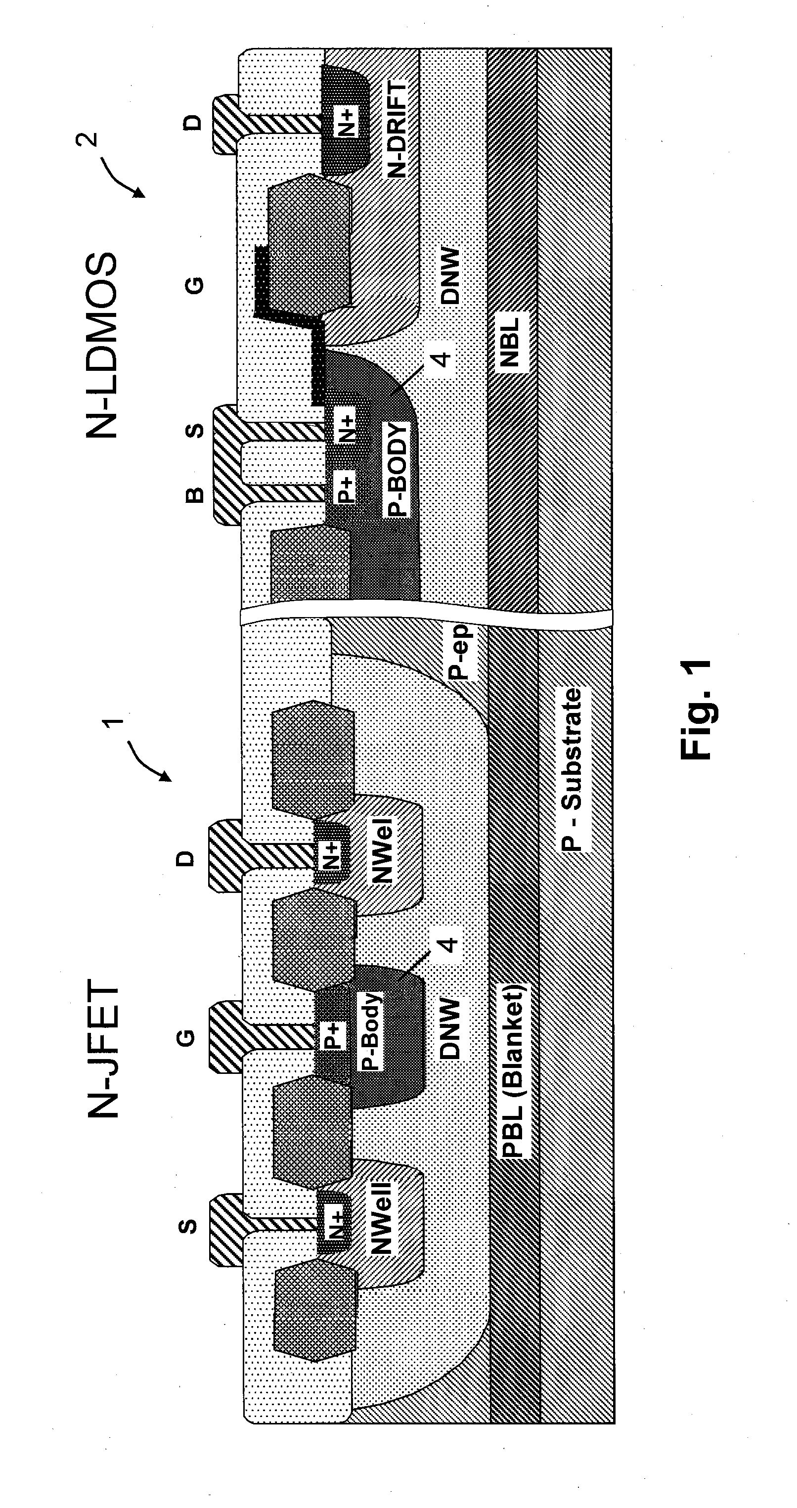
A power integrated circuit includes a junction field effect transistor (JFET) device formed in a first portion of a semiconductor layer with a gate region being formed using a first body region, and a double-diffused metal-oxide-semiconductor (LDMOS) transistor formed in a second portion of the semiconductor layer with a channel being formed in a second body region. The power integrated circuit includes a first deep diffusion region formed under the first body region and in electrical contact with the first body region where the first deep diffusion region together with the firs body region establish a pinch off voltage of the JFET device; and a second deep diffusion region formed under the second body region and in electrical contact with the second body region where the second deep diffusion region forms a reduced surface field (RESURF) structure in the LDMOS transistor.

Description

BACKGROUND OF THE INVENTION[0001]Monolithic power integrated circuits (PICs) for high-voltage applications may sometimes integrate thereon a junction field effect transistor (JFET) and a lateral double-diffused metal-oxide-semiconductor (LDMOS) transistor. For instance, a JFET device may be incorporated in a power integrated circuit to use as a normally on pass device for a startup circuit. The JFET device may have a drain terminal connected to a power source terminal (e.g. 12V), a gate terminal that is grounded, and a source terminal connected to a power supply node for a load. As the power source ramps up, the JFET conducts current in a channel between the drain and the source terminal to provide power to certain circuitry of the load. When the power supply node (source terminal) to the load reaches the desired power supply voltage for the load (e.g. 5V), the JFET channel is pinched off and the JFET device is turned off. JFET devices are preferred in the normally on pass device ap...

Claims


Application Information

Patent Timeline
Patent Type & Authority Applications(United States)
IPC IPC(8): H01L27/06H01L29/808H01L29/66H01L21/265H01L29/10H01L29/36H01L21/8232H01L29/78H01L29/06
CPCH01L29/7823H01L29/0878H01L29/66681H01L29/66901H01L29/36H01L21/8232H01L21/26513H01L29/1066H01L27/085H01L21/8234H01L29/7817H01L29/063H01L29/1095H01L29/42368H01L29/7816H01L29/808
Inventor MALLIKARJUNASWAMY, SHEKAR
Owner ALPHA & OMEGA SEMICON INC
Learn More