Silicon precursors for low temperature ald of silicon-based thin-films

Active Publication Date: 2015-05-28
ENTEGRIS INC
View PDF15 Cites 14 Cited by
  • Summary
  • Abstract
  • Description
  • Claims
  • Application Information

AI Technical Summary

Benefits of technology

The present patent relates to silicon precursors that can be used to deposit silicon-containing films by vapor deposition processes, and methods for making films using these precursors. The precursors can be silylene compounds, amidinate silylenes, or bis(amidinate) silylenes. The films can be used in microelectronic devices such as capacitors and ferroelectric field effect transistors. Additionally, the patent also describes a method for maintaining the amorphous character of certain materials during processing. Other aspects of the patent include methods for sealing porosity in a substrate with a silicon oxide film. The technical effects of the patent include improved deposition of silicon-containing films using vapor deposition processes and improved performance of microelectronic devices.

Problems solved by technology

The fundamental challenge in this effort is to achieve a balance of precursor thermal stability and precursor suitability for high-purity, low temperature film growth processes.

Method used


Image

  • Silicon precursors for low temperature ald of silicon-based thin-films
  • Silicon precursors for low temperature ald of silicon-based thin-films
  • Silicon precursors for low temperature ald of silicon-based thin-films

Examples


Embodiment Construction

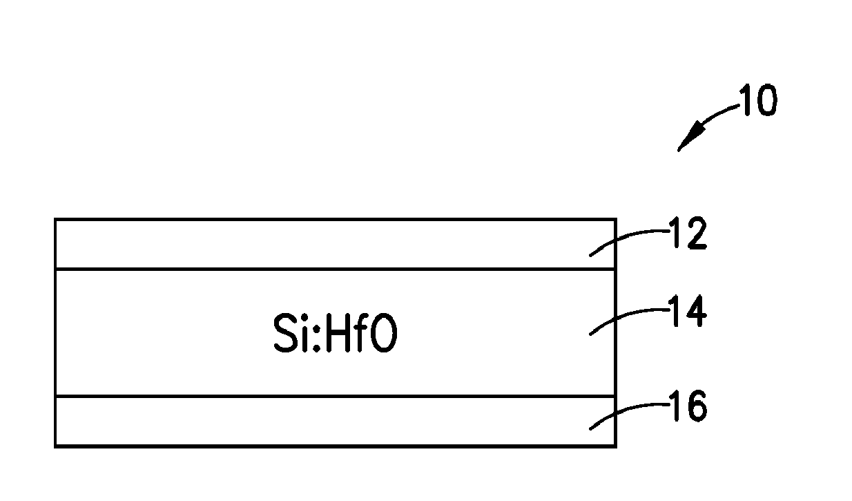
[0025]The present disclosure relates to silicon precursors that are amenable to use in low temperature vapor deposition processes such as CVD and ALD, to form silicon-based thin films.

[0026]As used herein, the term “film” refers to a layer of deposited material having a thickness below 1000 micrometers, e.g., from such value down to atomic monolayer thickness values. In various embodiments, film thicknesses of deposited material layers in the practice of the invention may for example be below 100, 10, or 1 micrometers, or in various thin film regimes below 200, 100, or 50 nanometers, depending on the specific application involved. As used herein, the term “thin film” means a layer of a material having a thickness below 1 micrometer.

[0027]It is noted that as used herein and in the appended claims, the singular forms “a”, “and”, and “the” include plural referents unless the context clearly dictates otherwise.

[0028]As used herein, the identification of a carbon number range, e.g., in C...


PUM

PropertyMeasurementUnit
Temperatureaaaaaaaaaa

Abstract

A silicon precursor composition is described, including a silylene compound selected from among: silylene compounds of the formula: wherein each of R and R1 is independently selected from organo substituents; amidinate silylenes; and bis(amidinate) silylenes. The silylene compounds are usefully employed to form high purity, conformal silicon-containing films of Si02, Si3N4, SiC and doped silicates in the manufacture of microelectronic device products, by vapor deposition processes such as CVD, pulsed CVD, ALD and pulsed plasma processes. In one implementation, such silicon precursors can be utilized in the presence of oxidant, to seal porosity in a substrate comprising porous silicon oxide by depositing silicon oxide in the porosity at low temperature, e.g., temperature in a range of from 50° C. to 200° C.

Description

CROSS-REFERENCE TO RELATED APPLICATIONS[0001]The benefit of priority under 35 USC 119 of U.S. Provisional Patent Application No. 61 / 652,010 filed on May 25, 2012 and the benefit of priority under 35 USC 119 of U.S. Provisional Patent Application No. 61 / 732,900 filed on Dec. 3, 2012 is hereby claimed. The disclosures of such related U.S. provisional applications are hereby incorporated herein by reference in their respective entireties, for all purposes.FIELD[0002]The present disclosure relates to silicon-based films for fabrication of microelectronic devices, and to silicon precursors useful in depositing such films by vapor deposition processes.DESCRIPTION OF THE RELATED ART[0003]Low temperature deposition of silicon-based thin-films is of fundamental importance to current semiconductor device fabrication and processes. For the last several decades, SiO2 thin films have been utilized as essential structural components of integrated circuits (ICs), including microprocessor, logic an...

Claims


Application Information

Patent Timeline
IPC IPC(8): H01L21/28H01L49/02C23C16/40C23C16/44C23C16/455H01L29/51C09D5/24
CPCH01L21/28229H01L29/516H01L28/40C23C16/401C23C16/44C23C16/45525C09D5/24C07F7/10C23C16/345C23C16/402
Inventor CAMERON, THOMAS M.DIMEO, SUSAN V.HENDRIX, BRYAN C.LI, WEIMIN
Owner ENTEGRIS INC
Why Eureka
Try Eureka