Random local metal cap layer formation for improved integrated circuit reliability

a technology of integrated circuit reliability and metal cap layer, which is applied in the direction of semiconductor devices, semiconductor/solid-state device details, electrical devices, etc., can solve the problems of electrical shorting of adjacent interconnects, increasing the width of interconnect lines, and increasing the risk of deleterious effects

Inactive Publication Date: 2015-01-29
GLOBALFOUNDRIES INC
View PDF1 Cites 0 Cited by
  • Summary
  • Abstract
  • Description
  • Claims
  • Application Information

AI Technical Summary

Problems solved by technology

As these integrated circuits are scaled to smaller dimensions in a continual effort to provide increased density and performance (e.g., by increasing device speed and providing greater circuit functionality within a given area chip), the interconnect line width dimension becomes increasingly narrow, which in turn renders them more susceptible to deleterious effects such as electromigration.
This in turn may lead to delamination, cracking, and even metal extrusion from the metal wire, thereby causing an electrical short to adjacent interconnects.
Moreover, as the CD shrinks, it also provides challenges for liner deposition.
Poor liner coverage will lead to the diffusion of the liner material, for example copper, to diffuse into the dielectric layer adjacent to it.
The destruction of the dielectric layer can cause interconnects to short, rendering the IC defective.
Unfortunately, steps taken to mitigate electromigration can adversely affect TDDB.

Method used


Image

  • Random local metal cap layer formation for improved integrated circuit reliability
  • Random local metal cap layer formation for improved integrated circuit reliability
  • Random local metal cap layer formation for improved integrated circuit reliability

Examples


Embodiment Construction

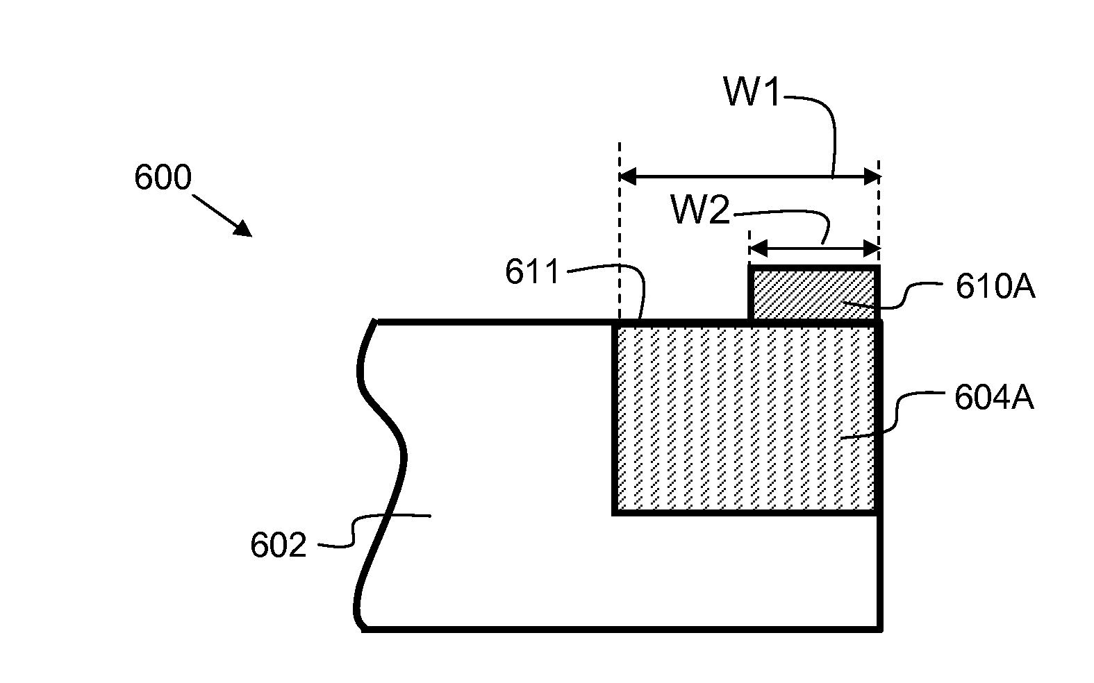
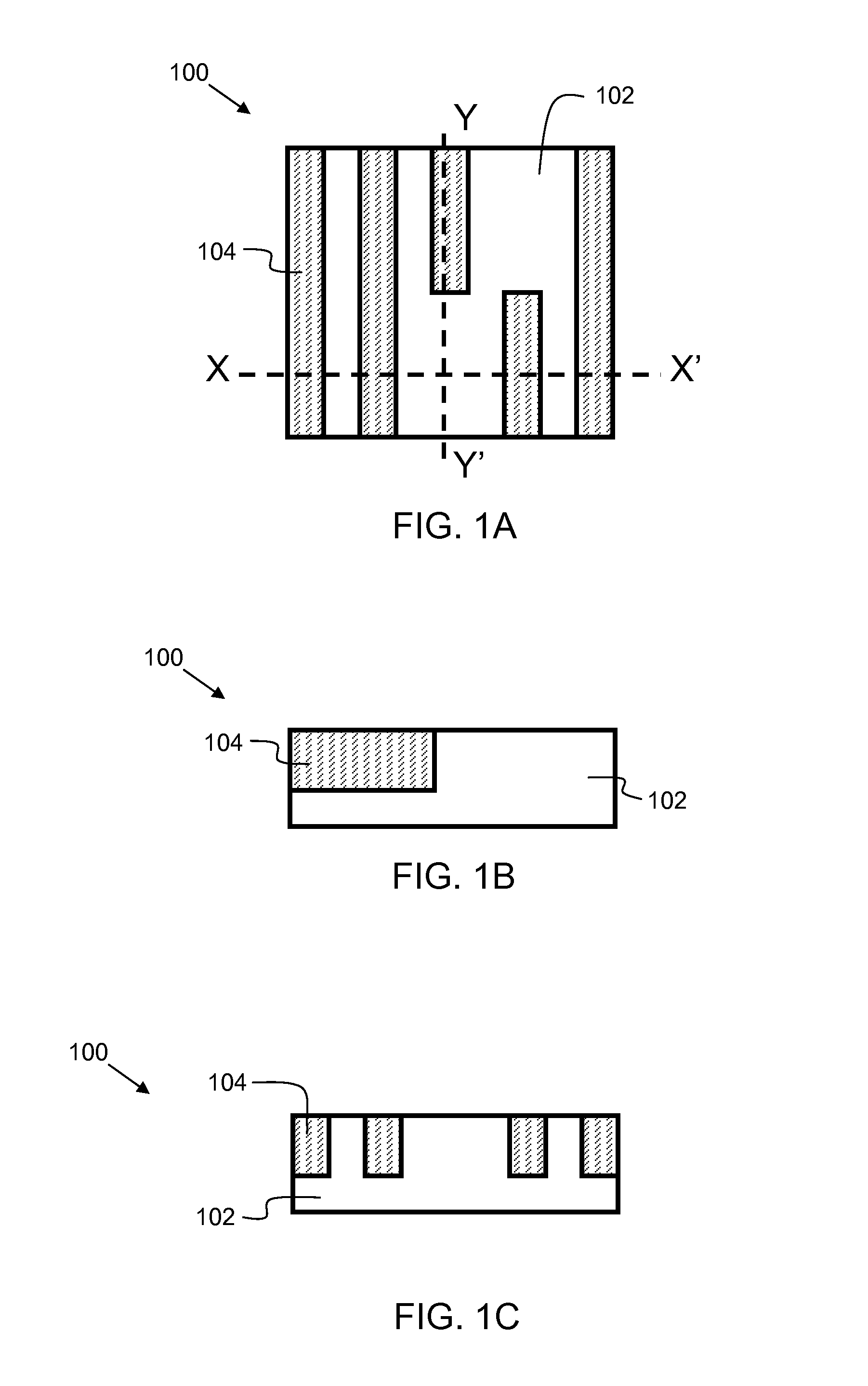
[0019]FIGS. 1A, 1B, and 1C show a semiconductor structure 100 at a starting point for embodiments of the present invention. FIG. 1A is a top-down view showing a semiconductor substrate 102 with a plurality of metal interconnect lines 104 formed thereon. The metal interconnect lines 104 may be comprised of copper, and may be formed by first etching a trench in semiconductor substrate 102, which may be an interlayer dielectric, and then filling the trench with the interconnect metal. FIG. 1B is a side view along line Y-Y′ of FIG. 1A. FIG. 1C is a side view along line X-X′ of FIG. 1A.

[0020]FIGS. 2A, 2B, and 2C show top and side views of a semiconductor structure 200 after a subsequent process step of forming a randomly oriented material on the substrate. This may comprise depositing a directed self-assembly (DSA) material. In embodiments, a spin-on coating process may be used to deposit the DSA material 206. As stated previously, similar elements may be referred to by similar numbers i...


PUM


Abstract

A method and structure for preventing integrated circuit failure due to electromigration and time dependent dielectric breakdown is disclosed. A randomly patterned metal cap layer is selectively formed on the metal interconnect lines (typically copper (Cu)) with an interspace distance between metal cap segments that is less than the critical length (for short-length effects). Since the diffusivity is lower for the Cu / metal cap interface than for the Cu / dielectric cap interface, the region with a metal cap serves as a diffusion barrier.

Description

FIELD OF THE INVENTION[0001]The present invention relates generally to semiconductor fabrication, and more particularly, to a metal cap layer and method of formation.BACKGROUND OF THE INVENTION[0002]Integrated circuits (ICs) are typically fabricated with multiple levels of patterned metallization lines, electrically separated from one another by interlayer dielectrics containing vias at selected locations to provide electrical connections between levels of the patterned metallization lines. As these integrated circuits are scaled to smaller dimensions in a continual effort to provide increased density and performance (e.g., by increasing device speed and providing greater circuit functionality within a given area chip), the interconnect line width dimension becomes increasingly narrow, which in turn renders them more susceptible to deleterious effects such as electromigration.[0003]Electromigration is a term referring to the phenomenon of mass transport of metallic atoms (e.g., copp...

Claims


Application Information

Patent Timeline
Patent Type & Authority Applications(United States)
IPC IPC(8): H01L23/528H01L23/532
CPCH01L23/528H01L23/53209H01L23/53242H01L23/53257H01L21/76838H01L23/53238H01L23/53261H01L21/76849H01L2924/0002H01L21/76834H01L2924/00
Inventor FILIPPI, RONALD G.KALTALIOGLU, ERDEMLI, WAI-KINWANG, PING-CHUANZHANG, LIJUAN
Owner GLOBALFOUNDRIES INC
Why Eureka
Try Eureka