
Method of manufacturing wiring board

a manufacturing method and wiring board technology, applied in the manufacture of lithographic masks, resist details, cable/conductors, etc., can solve the problems of high probability, damage to the electrical insulating property between the adjacent wiring conductors b>12/b>, and complicate the manufacturing process, so as to achieve the effect of simplifying the manufacturing process and reducing the risk of solder wettability

Inactive Publication Date: 2015-01-29
KYOCERA CIRCUIT SOLUTIONS
View PDF4 Cites 0 Cited by
  • Summary
  • Abstract
  • Description
  • Claims
  • Application Information

AI Technical Summary

Benefits of technology

The present invention provides a method of manufacturing a wiring board with high electrical insulating reliability between adjacent wiring conductors in a simple way. The method involves covering the side surface of the main conductor layer with a plating mask, which prevents the metal plating layer from attaching to the side surface of the main conductor layer and maintaining the electrical insulating interval between adjacent wiring conductors. The manufacturing process is simplified because only one etching process is necessary for the base metal layer portion where the main conductor layer is not attached.

Problems solved by technology

Therefore, in a case where the interval between the adjacent wiring conductors 12 is as narrow as 20 μm or less, it is highly likely that the electrical insulating property between the adjacent wiring conductors 12 is damaged by the solder which has wetted and spread to the side surface of the wiring conductor 12.
Furthermore, the etching process needs to be performed two times for a portion of the base metal layer 12a to which the main conductor layer 12b is not attached, which complicates the manufacturing process.

Method used


Image

  • Method of manufacturing wiring board
  • Method of manufacturing wiring board
  • Method of manufacturing wiring board

Examples


Embodiment Construction

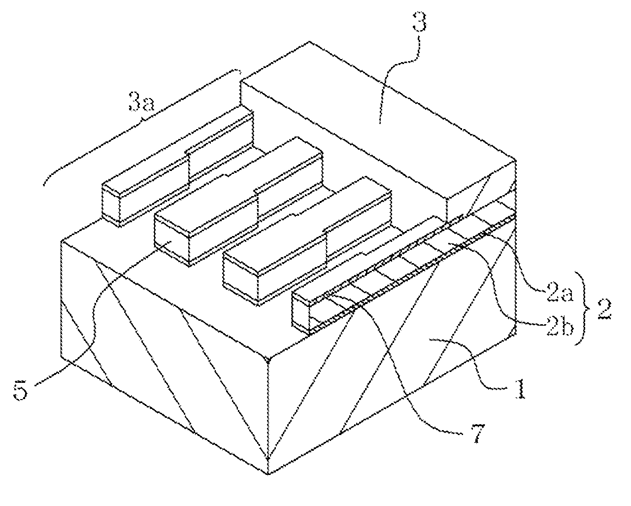
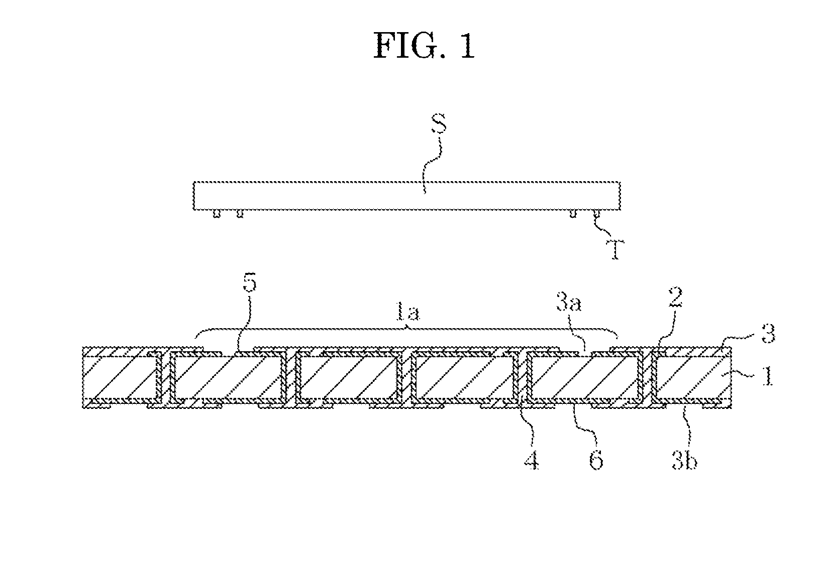
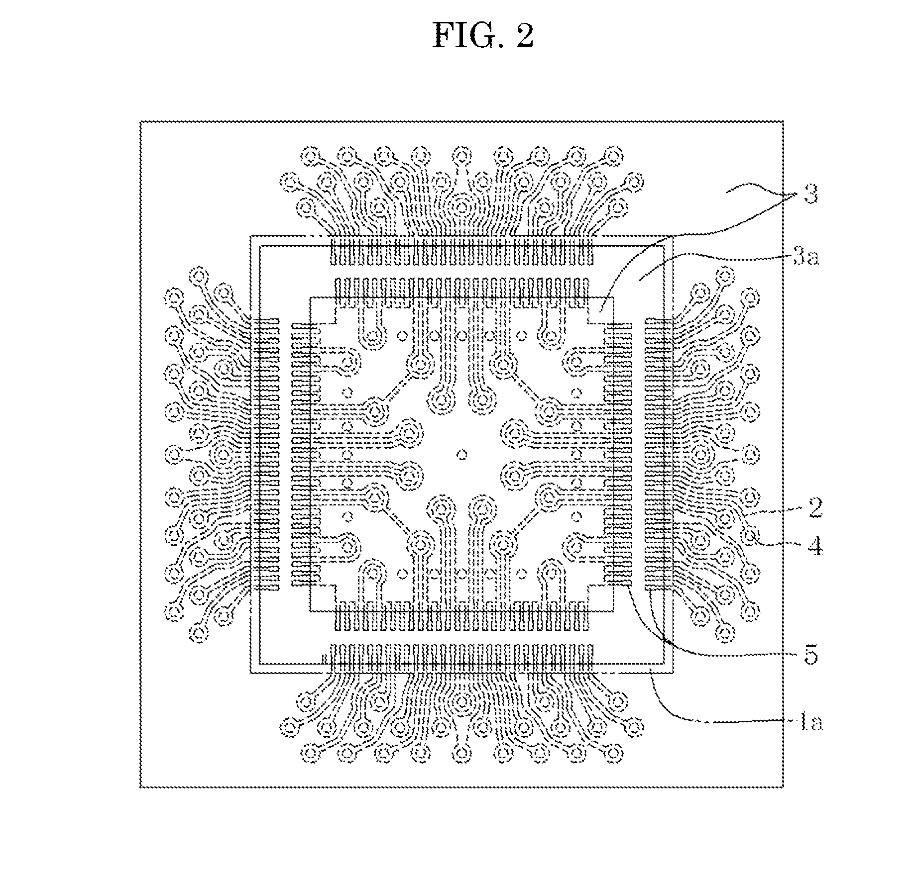
[0045]Next, the method of manufacturing the wiring board in the present invention will be described with reference to the accompanying drawings. FIG. 1 is a schematic cross-sectional view showing an example of the wiring board manufactured by the method in the present invention. FIG. 2 is a schematic top view of the wiring board shown in FIG. 1. FIG. 3 is an essential part enlarged cross-sectional view of the wiring board shown in FIG. 1.

[0046]This wiring board includes an insulating board 1, a wiring conductor 2, and a solder resist layer 3. In FIG. 2, broken lines show a portion of the wiring conductor 2 provided on an upper surface of the insulating board 1 and covered with the solder resist layer 3.

[0047]The insulating board 1 is composed of resin electrically insulating material formed by thermally curing a single or multiple insulating layers. The insulating layer is provided by impregnating a glass cloth base material with a thermoset resin such as epoxy resin or bismaleimide...


PUM


Abstract

A manufacturing method includes a step of forming a first plating mask on a base metal layer, a step of forming a main conductor layer on the base metal layer exposed from the first plating mask, a step of forming a second plating mask on them, a step of attaching a metal plating layer to an upper surface of the main conductor layer exposed from the second plating mask, a step of removing the first and second plating masks, a step of etching away a portion of the base metal layer to which the main conductor layer is not attached, and a step of forming a solder resist layer.

Description

BACKGROUND OF THE INVENTION[0001](1) Field of the Invention[0002]The present invention relates to a method of manufacturing a wiring board for mounting a semiconductor element such as a semiconductor integrated circuit element.[0003](2) Description of the Related Art[0004]The wiring board for mounting the semiconductor element has a copper wiring conductor for being electrically connected to the semiconductor element, on an upper surface of an insulating board. Furthermore, a solder resist layer is attached to the upper surface of the insulating board in such a manner that the wiring conductor which is electrically connected to the semiconductor element is partially exposed. In addition, a metal plating layer which is superior in solder wettability is attached to a surface of the wiring conductor which is exposed from the solder resist layer. Thus, an electrode of the semiconductor element is connected to the wiring conductor having the attached metal plating layer, with a solder. A...

Claims


Application Information

Patent Timeline
Patent Type & Authority Applications(United States)
IPC IPC(8): H05K3/06H05K3/07
CPCH05K3/061H05K3/07H05K2203/0582H05K2203/0548H05K2203/0369H05K3/108H05K3/243H05K3/244H05K3/3436H05K2201/09409H05K2203/0574H05K2203/0597
Inventor OHSUMI, KOHICHINOGUCHI, SUMIKO
Owner KYOCERA CIRCUIT SOLUTIONS
Learn More