Method for manufacturing a tool part for an injection molding process, a hot embossing process, a nano-imprint process, or an extrusion process

a technology of nano-imprinting and injection molding, which is applied in the direction of instruments, photomechanical treatment, optics, etc., can solve the problems of insufficient durability, unsatisfactory health or toxic, or rather complicated manufacturing, and achieve the effect of less complex and fast manufacturing

Inactive Publication Date: 2015-01-29
DANMARKS TEKNISKE UNIV +1
View PDF3 Cites 9 Cited by
  • Summary
  • Abstract
  • Description
  • Claims
  • Application Information

AI Technical Summary

Benefits of technology

[0015]Furthermore, an injection molding tool part according to the present invention can essentially manufacture final products in any thermoplastic material suitable for injection molding which may open up for wide spread application of the present invention, e.g. in every day consumer products already manufactured by injection molding.
[0016]In the context of the present invention, it is to be understood that the three options, (1, 2 and 3) for creation of protrusions:
[0017]1) alternating passivation and etching into the master structure, and / or
[0018]2) simultaneous passivation and etching into the master structure, and / or
[0019]3) etching into the master structure, can be applied solely (i.e. only option 1, 2 or 3), in combination (i.e. 1 and 2, or 1 and 3, or 1 and 3), such as a period of performing option 1 followed by another period with option 2, etc., and a combination of all 3 options (1, 2, and 3), such as various combination of periods with options 1, 2, and 3 for creation of protrusions, as the skilled person will readily understand once the general principle of the invention is comprehended.
[0020]Notice that the present invention applies various etching processes, which is quite different from US patent application 2007 / 115554 were the random protrusions are grown, typically over several hours. The present invention is typically order of magnitude faster and less complex to implement, in particular when implemented on a semiconductor wafer or similar in a cleanroom environment. In general, the present invention relates to a master structure made of a non-metal, such as a semiconductor material.

Problems solved by technology

Many consumer products today, use chemical coatings to lower adhesion or to repel water, these are potentially unhealthy or toxic.
Solutions are available but they are either rather complicated to manufacture due to the intensive need for lithographic processing , or they are not sufficiently durable over time, e.g. by being dependent on chemical coatings that are worn off during use.
Some chemical coatings used in consumer products today use e.g. fluorine containing chemical coatings, which are potentially unhealthy or toxic.
The production of the master structure is however quite time consuming due to the intensive need for complex, and therefore costly, lithography steps for designing the proposed mathematical structures resulting in a lotus-like functionality in the final product.
The growth of such protrusions is typically somewhat time-consuming thereby representing a bottle neck for manufacturing use.

Method used


Image

  • Method for manufacturing a tool part for an injection molding process, a hot embossing process, a nano-imprint process, or an extrusion process
  • Method for manufacturing a tool part for an injection molding process, a hot embossing process, a nano-imprint process, or an extrusion process
  • Method for manufacturing a tool part for an injection molding process, a hot embossing process, a nano-imprint process, or an extrusion process

Examples


Embodiment Construction

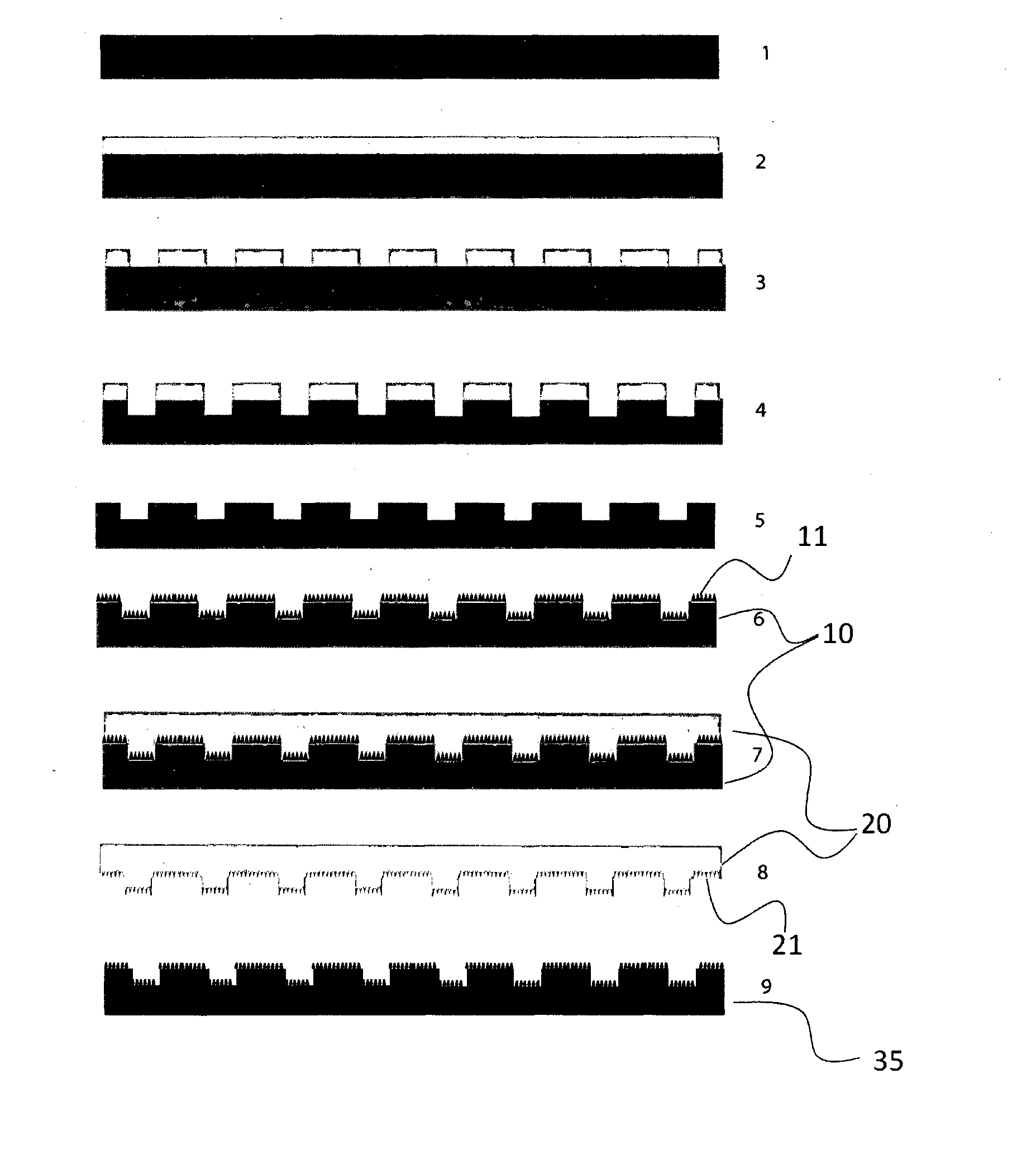
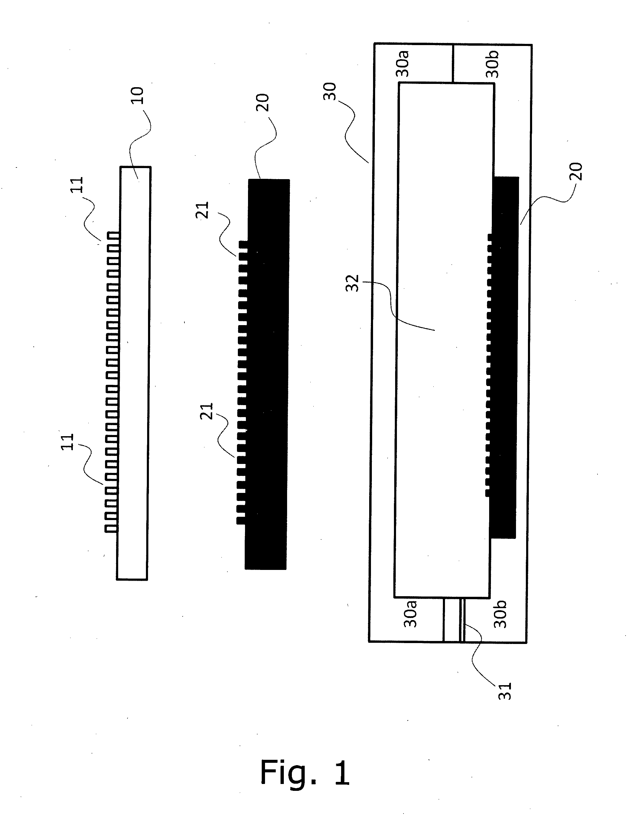
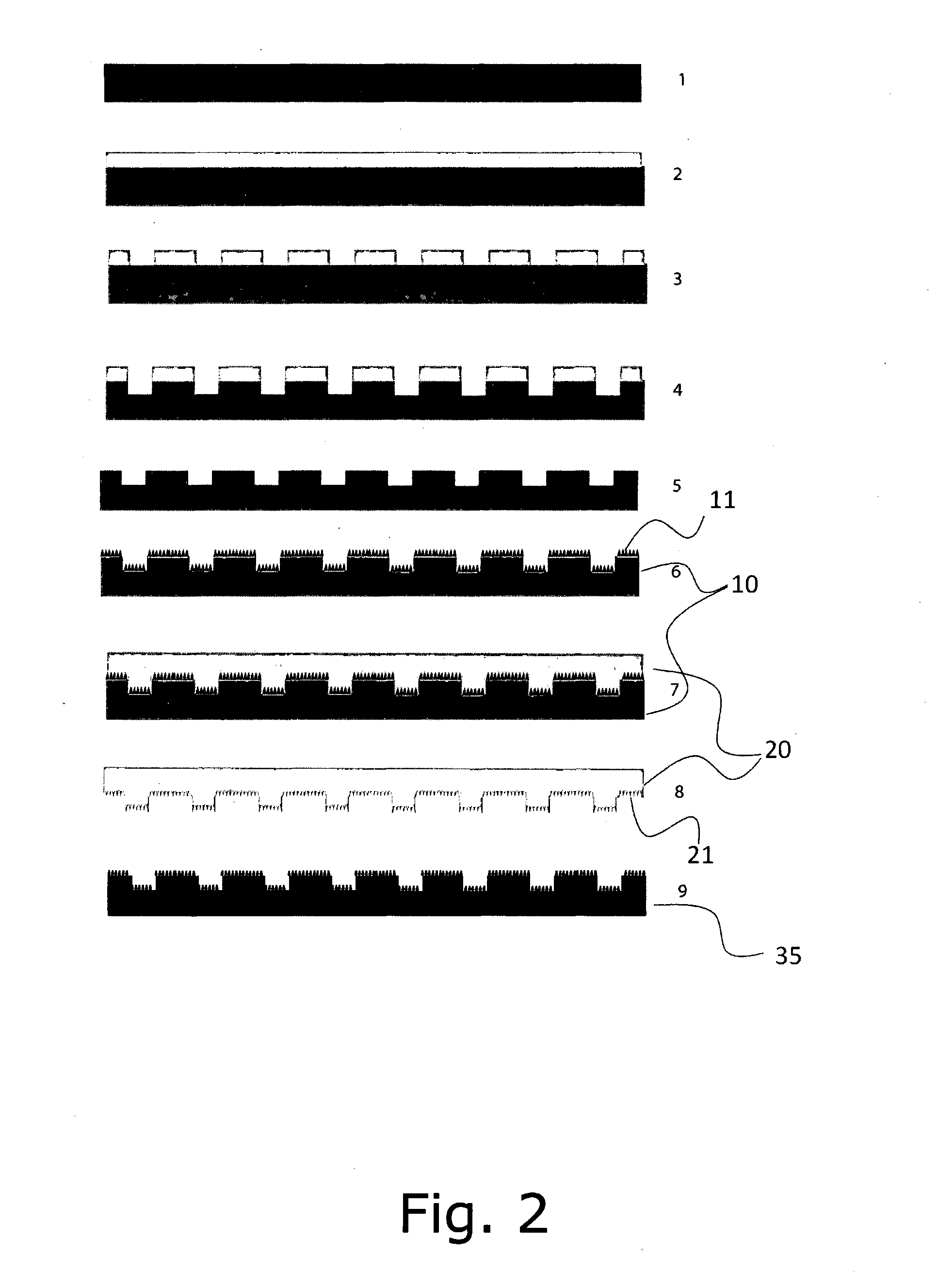
[0065]FIG. 1 shows a schematic overview of the three main steps forming part of the invention; providing a master structure 10, transferring to a metal insert 20, and adapting to a tool part 30.

[0066]The master structure 10 has a surface area comprising nanometre-sized protrusions 11 (not to scale) with a minimum density of approximately 105 protrusions / mm2, the protrusions being positioned in a non-periodic, irregular pattern i.e. essentially a random or non-deterministic pattern, said protrusions being created by a process comprising:[0067]1) alternating passivation and etching into the master structure, e.g. reactive ion etching by the so-called Bosch method, and / or[0068]2) simultaneous passivation and etching into the master structure, e.g.

[0069]reactive ion etching by the so-called cryogenic method, and / or[0070]3) etching into the master structure, e.g. by a chemical wet etching.

[0071]Subsequently, the pattern of the protrusions 11 is transferred from the master structure 10 in...


PUM

PropertyMeasurementUnit
sizeaaaaaaaaaa
aspect ratioaaaaaaaaaa

Abstract

The present invention relates to a method for manufacturing a tool part for an injection molding process, a hot embossing process, nano-imprint process or an extrusion process. First, there is provided a master structure (10) with a surface area comprising nanometre-sized protrusions (11) with a minimum density of approximately 105 protrusions/mm2, the protrusions being positioned in a non-periodic, irregular pattern, said protrusions being created by a process comprising alternating passivation and etching into the master structure. Secondly, there is made a transfer of the master structure into a metal insert (20), the metal insert having a corresponding nanometre-sized pattern (21) from said protrusions, and thirdly, adapting the metal insert into a tool part (30) for enabling nanometre-sized patterns being formed by the tool part. The invention provides an easier and faster way of manufacturing the master structure, e.g. a black silicon wafer. It is a further advantage of the present invention that it provides an advant ageous way of making tools capable of producing self-cleaning surfaces without the need for chemical coating.

Description

FIELD OF THE INVENTION[0001]The present invention relates to a method for manufacturing a tool part for an injection molding process, a hot embossing process, a nano-imprint process, or an extrusion process. The invention also relates to corresponding tool part, e.g. a tool part capable of producing a self-cleaning surface in an object.BACKGROUND OF THE INVENTION[0002]Injection molded polymer parts with micro- or nano-structured surfaces, has the ability to introduce wide range of new functionalities. Many consumer products today, use chemical coatings to lower adhesion or to repel water, these are potentially unhealthy or toxic. Surfaces with self-cleaning nano and microstructures that imitate the lotus flower. This is of high relevance for the medical and food producing industries. For example, medical and food containers can be designed so they can be completely emptied. Therefore, none of the expensive medicine or food is wasted. Furthermore, self-cleaning surfaces are relevant ...

Claims


Application Information

Patent Timeline
Patent Type & Authority Applications(United States)
IPC IPC(8): B29C33/38B29C33/72B29C33/42
CPCB29C33/3878B29C33/424B29C2033/426B29C2033/3864B29C33/72G03F7/0002B29C45/372B29C33/3857B82Y10/00B82Y40/00B29C45/263B29C33/42Y10T29/49885
Inventor TABORYSKI, RAFAELSOGAARD, EMILSMISTRUP, KRISTIAN
Owner DANMARKS TEKNISKE UNIV
Why Eureka
Try Eureka