
Method of global design closure at top level and driving of downstream implementation flow

a global design and implementation flow technology, applied in the field of top-down design methods and systems, can solve the problems of large and complex socs of the day, ips typically end up having complexities similar, and limited access and knowledge of the internal structure of the ip

Active Publication Date: 2014-10-02
SYNOPSYS INC
View PDF1 Cites 22 Cited by
  • Summary
  • Abstract
  • Description
  • Claims
  • Application Information

AI Technical Summary

Benefits of technology

The patent describes a method for designing the placement and timing of components in a semiconductor device. The method allows for efficient placement and routing of components, reducing congestion and improving timing. The method also enables early back-end optimization to address any remaining issues in the design. Overall, this method helps to close the design and improve the performance of the semiconductor device.

Problems solved by technology

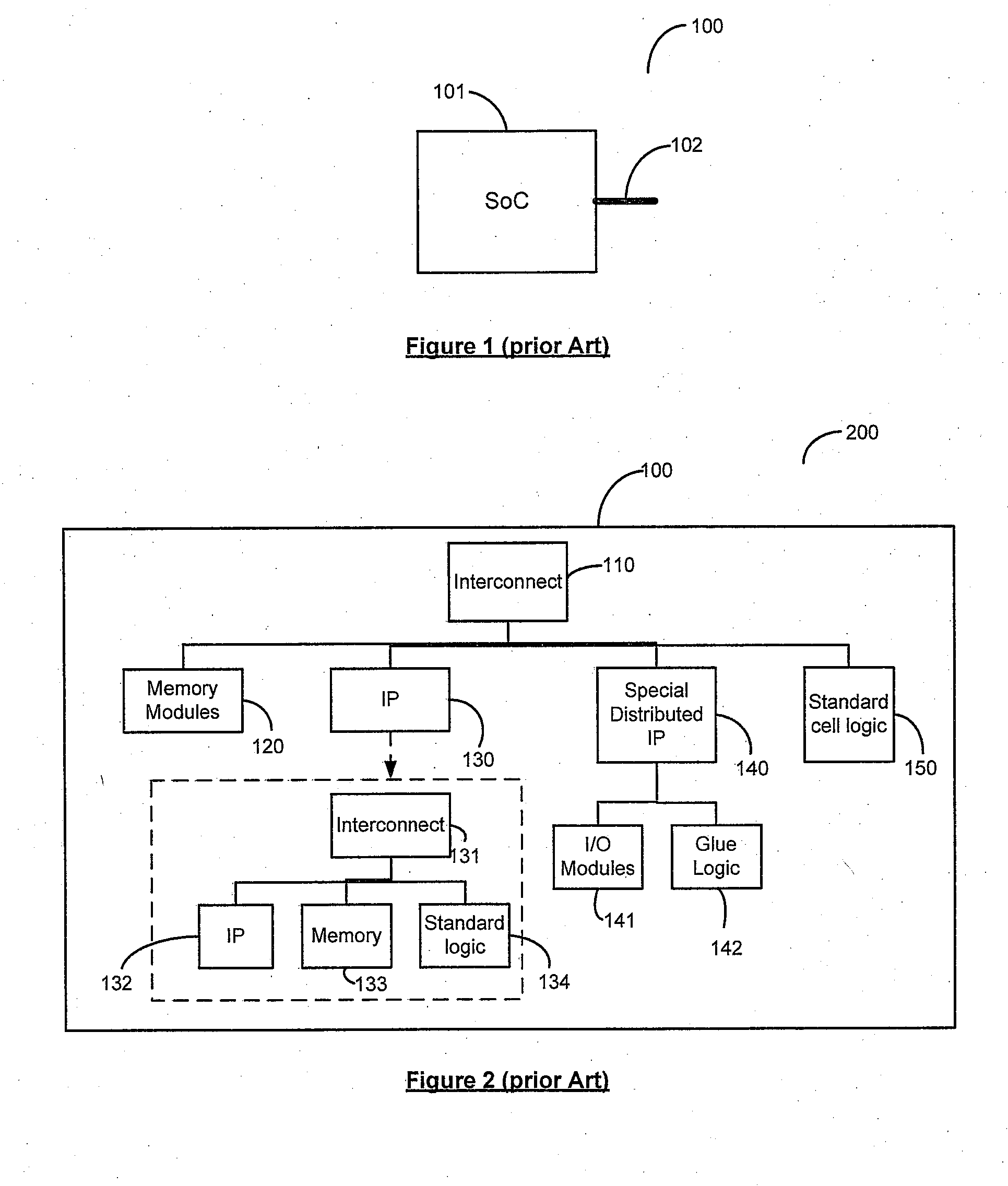
Today's SoCs are very large and complex with large number of IP blocks, memory blocks, and logic connected using one or more interconnect bus fabric.
These IPs typically end up having complexities similar to the SoC itself but on a smaller scale, in that these can have 10 s of millions of placeable instances, hundreds of memory blocks or macros, multiple clock trees with differing clock frequencies and multiple power domains.
The teams that work on hardening and design closure of the IPs and SoCs typically are different from the RTL designers and have limited access and knowledge of the internal structure of the IP.
This makes the process of design closure very complex and time consuming.
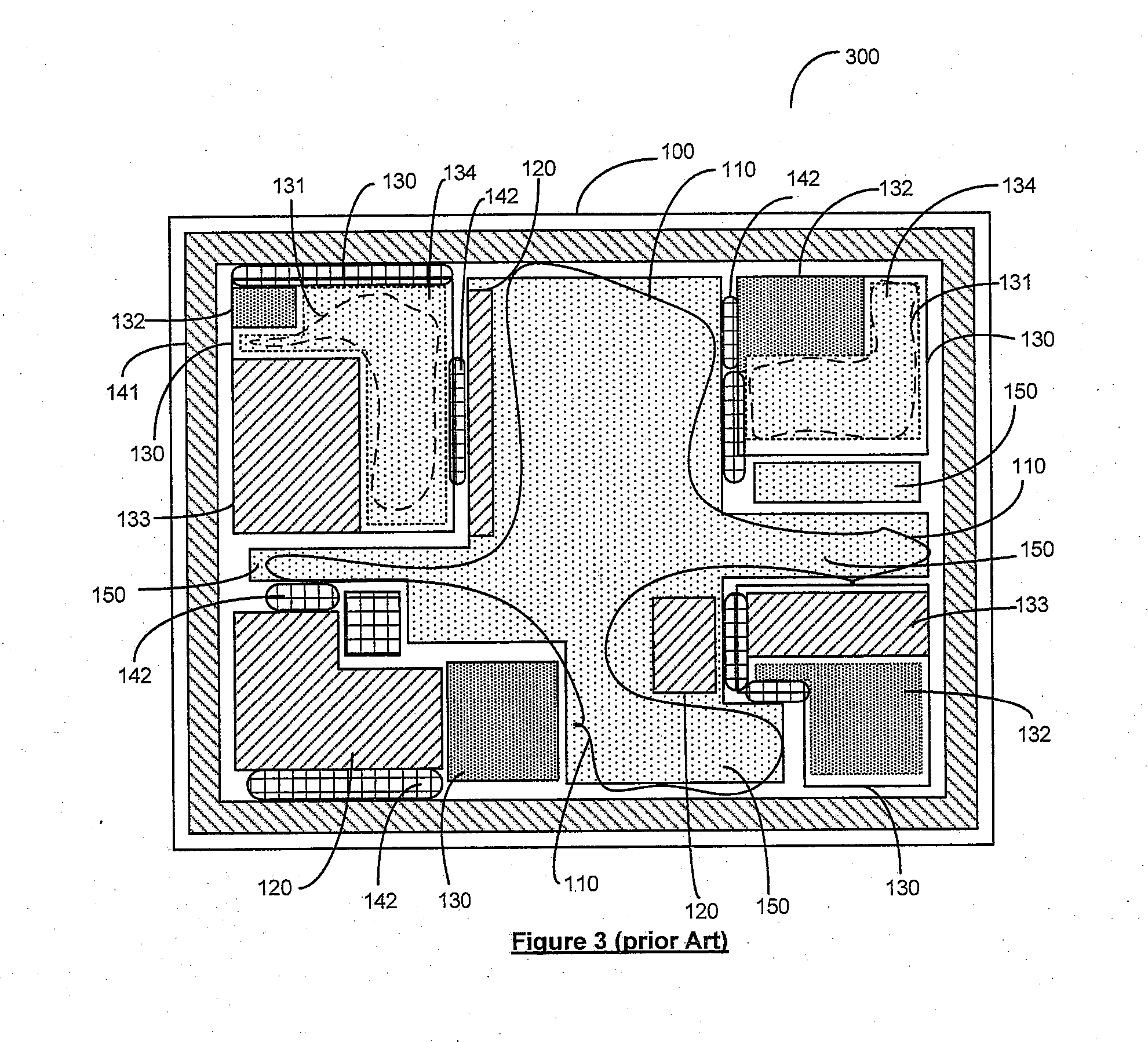
The current circuit design flows typically do not allow design closure and validation before the detailed place and route is complete even though the critical paths are typically the global routes within the SoC 100.
Though there have been programs that enable wire modeling providing delay estimates of interconnects, these have not been accurate enough to provide estimates that are realistic below 45 nm technology node as the wiring parasitic dominate the delays.
This makes it impossible to have design closure and validation without completing the final physical planning and place and route of the SoC 100.

Method used


Image

  • Method of global design closure at top level and driving of downstream implementation flow
  • Method of global design closure at top level and driving of downstream implementation flow
  • Method of global design closure at top level and driving of downstream implementation flow

Examples


Embodiment Construction

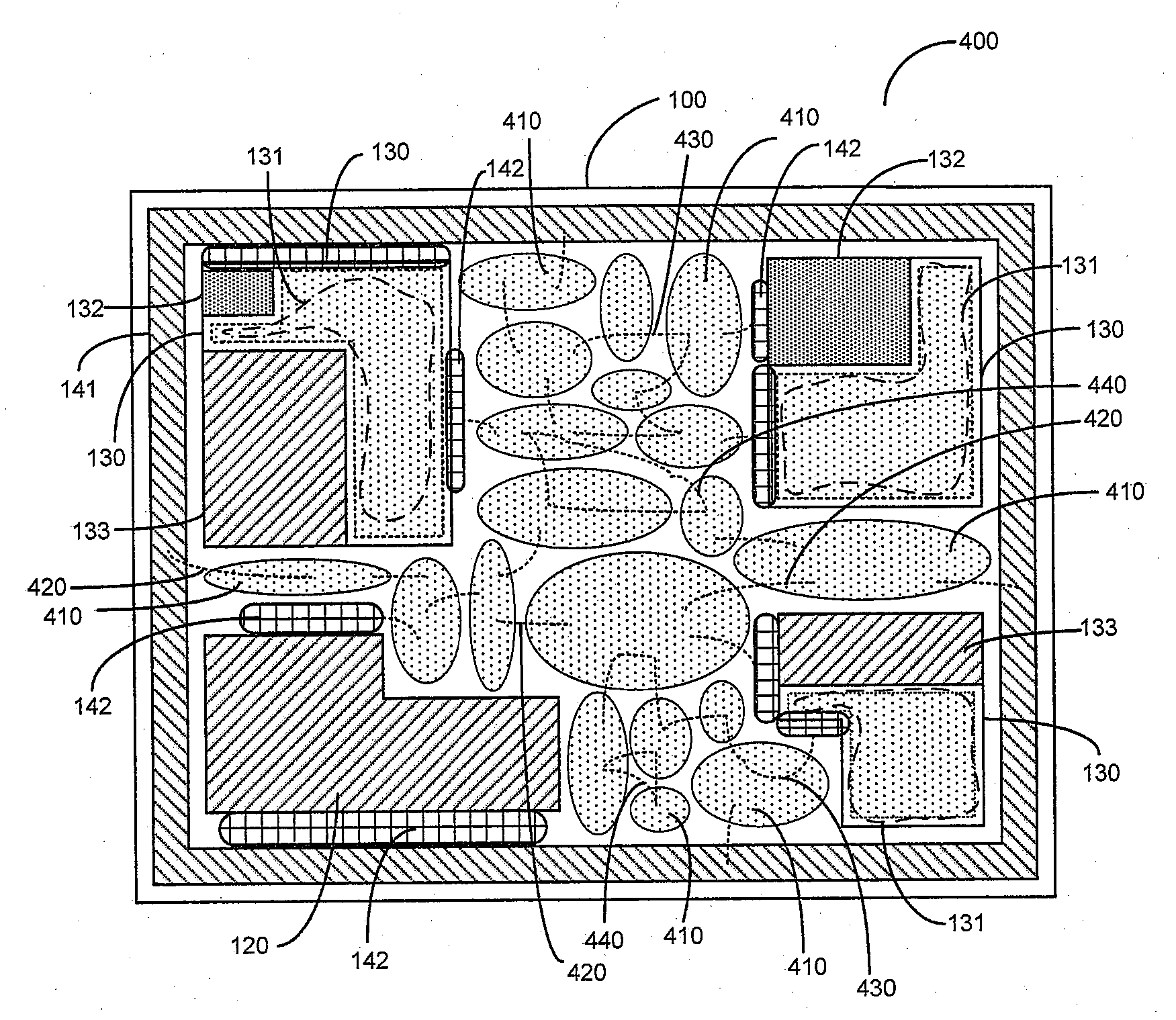
[0020]System-on-chip (SoC) 100 designs include large amount of interconnected intellectual property (IP) blocks 130, memory 120 and standard-cell logic 150, using complex bus fabrics 110. The IP blocks 130 are customized or hardened to the target constraints of SoC design 101 by fixing the core dimensions and shapes. Today SOC design-closure that validates design targets of area, timing, congestion and power constraints are accomplished post routing as a majority of validation problems are due to global-interconnect. This iterative and time consuming validation process towards the tail end of design cycle extends the design time and cost of design of the SOC.

[0021]A system and method are disclosed that allow the designers to achieve global design-closure and physical topology constraints, early in the design cycle, at much higher levels of abstraction. Using the results of this top-down global design-closure method the designers can guide the downstream, tools to achieve predictable...


PUM


Abstract

System-on-chip (SoC) designs include large amounts of interconnected intellectual property blocks and standard-cell logic using complex bus fabrics. Today SoC design-closure that validates design targets of area, timing, congestion and power constraints is accomplished post routing as over 80% of validation problems are due to global-interconnect. A method is disclosed that allows the designers to achieve global design-closure and physical topology constraints, early in the design cycle, at much higher levels of abstraction. In particular, logic hierarchy of the design is converted into a physical hierarchy of functional-related clusters of locally-connected logic. The clusters and inter-cluster global connections can be refined to meet design constraints in order to generate a top-level floor-plan in the form of library and constraint files. Using the results of this top-down global design-closure method the designers can use the generated floor-plan to guide downstream tools to achieve predictable and correlatable design implementation.

Description

CROSS-REFERENCE TO RELATED APPLICATION[0001]This patent application claims priority under 35 U.S.C. 119(e) from prior U.S. provisional application No. 61 / 806,906, filed Mar. 31, 2013.TECHNICAL FIELD[0002]The present invention relates to systems and methods for completing design closure for system-on-chip (SoC) integrated circuits. The invention specifically relates to a top-down design method and system that allows for fast and efficient design closure, while meeting area, timing, congestion and power constraints, by enabling physical planning early in the design cycle of the SoC.BACKGROUND ART[0003]Today's SoCs are very large and complex with large number of IP blocks, memory blocks, and logic connected using one or more interconnect bus fabric. Many of the IP blocks are third party IPs with RTLs licensed from vendors. These base IPs are then customized or hardened to suit the use in the SoC by instantiation of additional memory blocks, adding pipelining to speed up the operation, ...

Claims


Application Information

Patent Timeline
Patent Type & Authority Applications(United States)
IPC IPC(8): G06F17/50
CPCG06F17/5045G06F30/30G06F30/327G06F2115/08G06F2119/12G06F2115/02
Inventor VARADARAJAN, RAVIGUPTA, JITENDRAMATHUR, SANJIVMITTAL, PRIYANKPATHAK, KAUSHAL KISHOREKRISHNA, KSHITIZNAGRATH, ANUPMITTAL, RITESH
Owner SYNOPSYS INC
Learn More