
Organic Light Emitting Diode Display Device and Method for Manufacturing the Same

Active Publication Date: 2014-10-02
LG DISPLAY CO LTD
View PDF7 Cites 60 Cited by
  • Summary
  • Abstract
  • Description
  • Claims
  • Application Information

AI Technical Summary

Benefits of technology

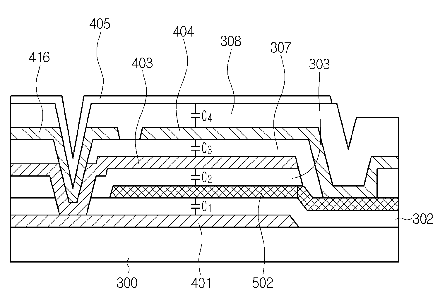
The present patent application is directed to an OLED device and a manufacturing method thereof that address limitations and disadvantages of related art. The technical effects of the patent include providing a switching element with a high speed response property by forming thin film transistors with a dual gate structure in a pixel region, and realizing a larger storage capacitance compared to an occupation area within a pixel region by stacking a plurality of storage electrodes. These technical effects improve the performance and efficiency of the OLED device.

Problems solved by technology

As such, it is difficult for the pixel region to secure a sufficient aperture ratio.

Method used


Image

  • Organic Light Emitting Diode Display Device and Method for Manufacturing the Same
  • Organic Light Emitting Diode Display Device and Method for Manufacturing the Same
  • Organic Light Emitting Diode Display Device and Method for Manufacturing the Same

Examples


Embodiment Construction

[0033]Reference will now be made in detail to the embodiments of the present disclosure, examples of which are illustrated in the accompanying drawings. These embodiments introduced hereinafter are provided as examples in order to convey their spirits to the ordinary skilled person in the art. Therefore, these embodiments might be embodied in a different shape, so are not limited to these embodiments described here. Also, the size and thickness of the device might be expressed to be exaggerated for the sake of convenience in the drawings. Wherever possible, the same reference numbers will be used throughout this disclosure including the drawings to refer to the same or like parts.

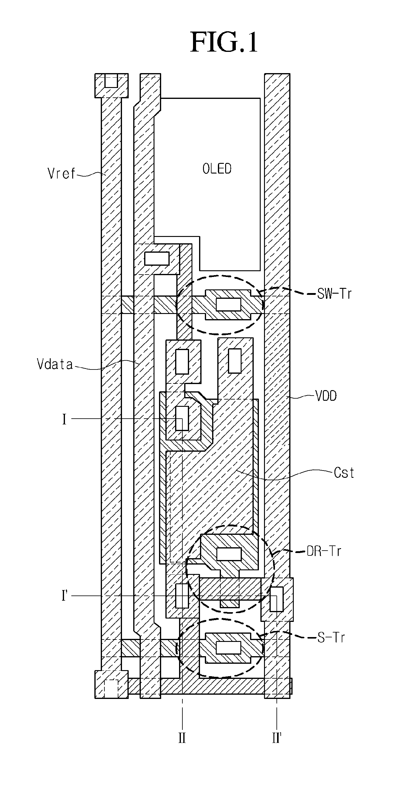
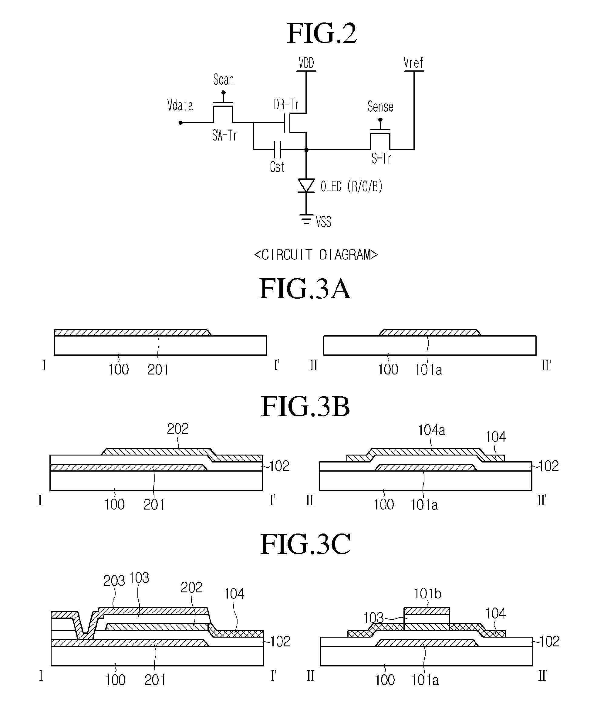
[0034]FIG. 1 is a planar view showing the pixel structure of an OLED device according to an embodiment of the present disclosure. FIG. 2 is an equivalent circuit diagram showing the pixel structure of FIG. 1.

[0035]Referring to FIGS. 1 and 2, the OLED device defines a plurality of pixel regions arranged in a...


PUM


Abstract

An organic light emitting diode display device is disclosed which includes: scan, data and power lines crossing one another and arranged to define a pixel region; a switching thin film transistor disposed at an intersection of the scan and data lines; an organic light emitting diode disposed in the pixel region; a driving thin film transistor disposed between the power line and the organic light emitting diode; and a storage capacitor disposed adjacently to the organic light emitting diode and configured to charge a data signal which is applied from the data line. The storage capacitor includes a plurality of sub storage capacitors in which a plurality of storage electrodes are stacked alternately with one another.

Description

[0001]The present application claims priority under 35 U.S.C. §119(a) of Korean Patent Application No. 10-2013-0031852 filed on Mar. 26, 2013 and Korean Patent Application No. 10-2013-0090778 filed on Jul. 31, 2013, which are hereby incorporated by reference in their entirety.BACKGROUND[0002]1. Field of the Disclosure[0003]The present application relates to an organic light emitting diode display device and a method of manufacturing the same.[0004]2. Description of the Related Art[0005]Recently, flat panel display devices with reduced weight and volume corresponding to disadvantages of cathode ray tube (CRT) are being developed. The flat panel display devices include liquid crystal display (LCD) devices, field emission display (FED) devices, plasma display panels (PDPs), organic light emitting diode display (OLED) devices and so on.[0006]The OLED device is a self-luminous device which uses a thin light emission layer between electrodes. As such, the OLED device can become thinner th...

Claims


Application Information

Patent Timeline
IPC IPC(8): H01L27/32
CPCH01L27/3265H01L27/3262H01L27/1225H01L27/1255H01L29/78648H10K59/1213H10K59/1216H10K71/231H10K71/00H10K71/166H01L27/1259
Inventor KIM, YOUNG JUNCHO, BO KYOUNG
Owner LG DISPLAY CO LTD
Learn More