
Package, electronic device, method of manufacturing electronic device, electronic apparatus, and moving object

a technology of electronic devices and manufacturing methods, applied in the direction of sealing, coupling device connections, rigid containers, etc., can solve the problems of difficult external inspection to confirm the sealing state, the quality of an electronic device may not be maintained, and the portion in which the member is heated is limited, so as to achieve high reliability

Active Publication Date: 2014-10-02
SEIKO EPSON CORP
View PDF7 Cites 9 Cited by
  • Summary
  • Abstract
  • Description
  • Claims
  • Application Information

AI Technical Summary

Benefits of technology

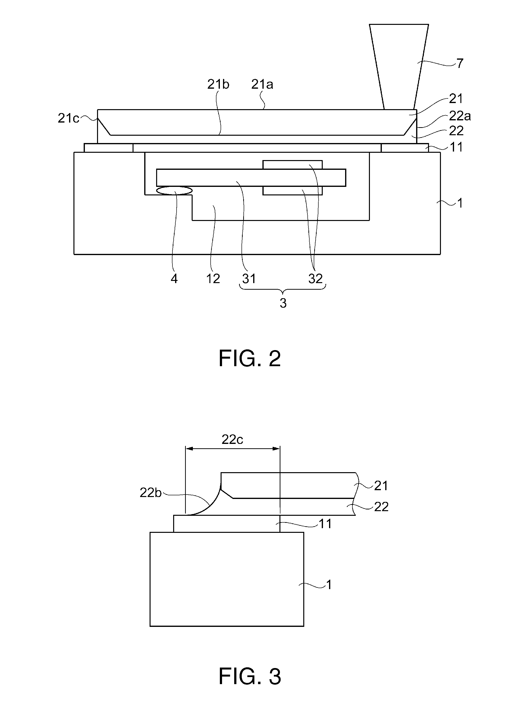
The patent text describes a method of manufacturing a lid with a brazing material layer that is melted and flows out to join the metalized layer and the outer peripheral side surface of the metal plate layer, forming a fillet of brazing material that strengthens the seal and prevents contamination. The brazing material layer is formed over the entire surface of the lid and has a protruding shape that flows out to both sides of the metalized layer, resulting in a stronger joining of the base portion and the lid. The method also reduces costs by using a protruding shape that can be easily formed without increasing the number of processes. Overall, the method provides a reliable and airtight inner space for the package.

Problems solved by technology

Furthermore, in the package structure disclosed in JP-A-2005-142329, since the fillet 604 of the brazing material 603b is not likely to be formed over the entire outer peripheral portion of the metal plate 603a, it is difficult to confirm a sealing state in an external inspection.
Thus, there is a concern that the quality of an electronic device may not be maintained since it is very difficult to determine whether or not the sealing state is satisfactory in the package structure disclosed in JP-A-2005-142329.
In addition, since the base portion and the lid are joined by welding in which only the brazing material layer provided around the metalized layer is melted, a portion in which the member is heated is limited only to the vicinity to be joined.

Method used


Image

  • Package, electronic device, method of manufacturing electronic device, electronic apparatus, and moving object
  • Package, electronic device, method of manufacturing electronic device, electronic apparatus, and moving object
  • Package, electronic device, method of manufacturing electronic device, electronic apparatus, and moving object

Examples


embodiment

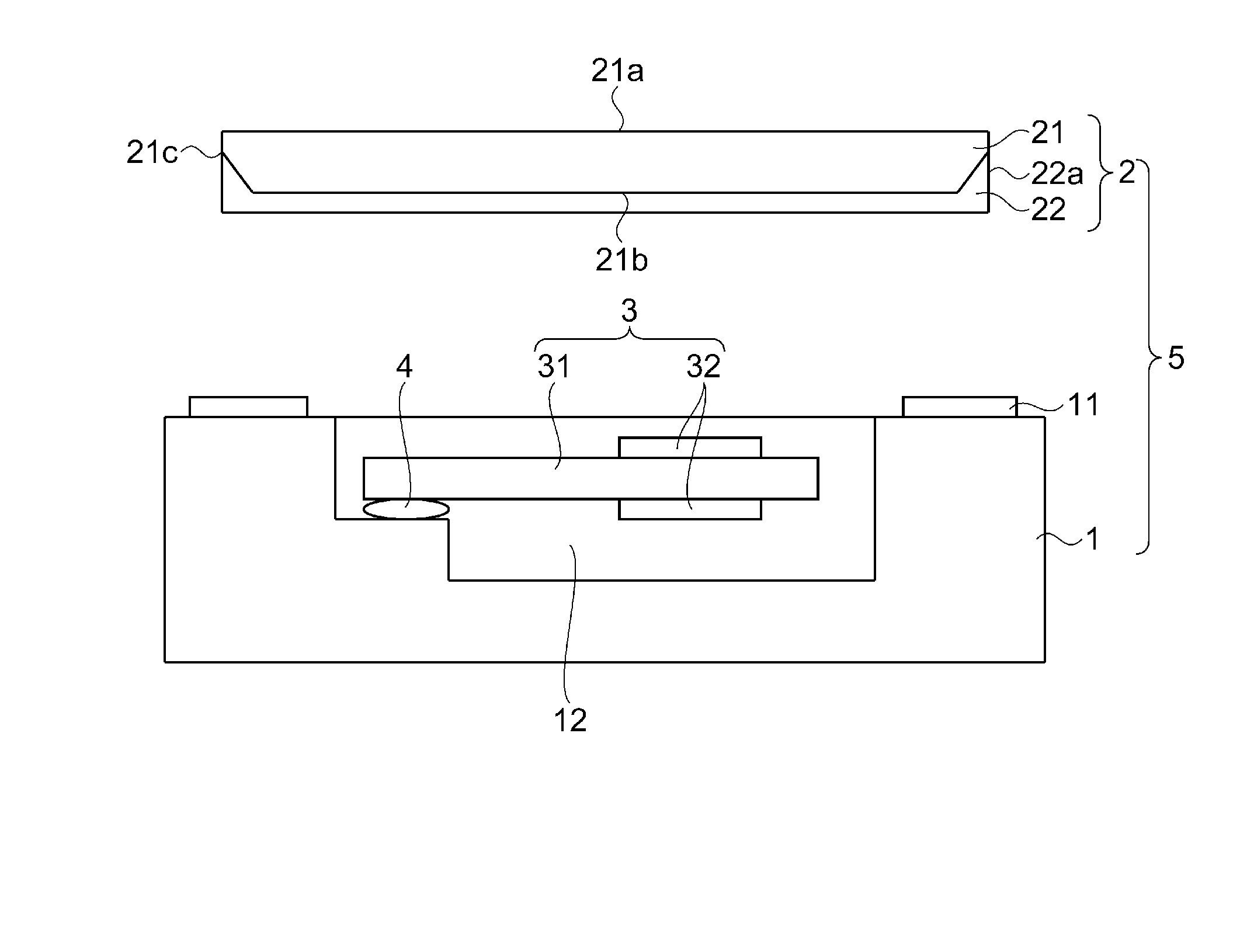
[0045]FIG. 1 is a cross-sectional view showing a schematic configuration of a resonator (a quartz crystal resonator) as an example of an electronic device according to an embodiment.

[0046]As shown in FIG. 1, the quartz crystal resonator 5 includes a base portion 1, a metalized layer 11, a quartz crystal resonator element 3 as an electron element, a lid 2, and the like.

[0047]The base portion 1 is formed of an insulator such as an aluminum oxide sintered body obtained by molding, laminating, and firing a ceramic green sheet, and the like and has a recessed portion 12 inside.

[0048]The metalized layer 11 is arranged on the joining surface of the base portion 1 with the lid 2, and the metalized layer 11 is formed of a metal coating film obtained by laminating an underlying metal such as tungsten or molybdenum and laminating a metal such as nickel, or gold on the underlying metal by plating, sputtering, and vapor deposition. Here, it is preferable that a surface layer metal of the metaliz...

modification example 1

[0064]FIG. 4 is a cross-sectional view of Modification Example 1 of the lid 2.

[0065]Here, the same signs are assigned to the same parts as in the above-described embodiment, and thus the description thereof will be omitted.

[0066]As shown in FIG. 4, in the metal plate layer 21 of the lid 2 according to the modification example, the corner portions of the surface 21b of the metal plate layer 21 close to the brazing material layer and the outer peripheral side surface 21c are chamfered in a curved-surface shape and the brazing material layer 22 has the protrusion 22a of the brazing material layer that protrudes toward the outer surface 21a which is a surface in a opposite direction of the base portion 1 on the outer peripheral side surface 21c of the metal plate layer 21. At this time, since there are no right angle and acute angle on the path from the surface 21b of the metal plate layer 21 close to the brazing material layer to the outer peripheral side surface 21c, the surface 21b c...

modification example 2

[0068]FIG. 5 is a cross-sectional view of Modification Example 2 of the lid 2.

[0069]Here, the same signs are assigned to the same parts as in the above-described embodiment, and thus the description thereof will be omitted.

[0070]The lid 2 of the modification example is formed in such a manner that the brazing material layer 22 is formed on one surface of a metal plate which is larger than the metal plate layer 21, and then, the lid is cut from the brazing material layer through a punching process from the brazing material layer 22. When the lid 2 is formed in such a manner, as shown in FIG. 5, the brazing material layer 22 is stretched to the outer peripheral side surface 21c of the metal plate layer 21 during the punching process, and thus, it is possible to form the protrusion 22a of the brazing material layer 22 which protrudes toward the outer surface 21a, which is a surface in an opposite direction of the base portion 1 on the outer peripheral side surface 21c of the metal plat...


PUM

PropertyMeasurementUnit
Widthaaaaaaaaaa

Abstract

A package includes a base portion, and a lid which is placed on the base portion to define an inner space with the base portion and has a metal plate layer and a brazing material layer that is laminated on the metal plate layer, in which the base portion has a metalized layer which is joined with the brazing material layer around the inner space in a plane view, and the brazing material layer has a protrusion which protrudes in a opposite direction of the base portion on an outer peripheral side surface of the metal plate layer.

Description

BACKGROUND[0001]1. Technical Field[0002]The present invention relates to a package, an electronic device including the package, an electronic apparatus, a moving object, and a method of manufacturing an electronic device.[0003]2. Related Art[0004]In recent years, in various communication devices, and particularly, in mobile communication devices, there has been a strong demand for reduction in size for an electronic device. As electronic devices used in the mobile communication devices, there are a piezoelectric resonator, a piezoelectric oscillator, a piezoelectric sensor, a SAW filter, and the like.[0005]In the piezoelectric devices whose size reduction is demanded as mentioned above, a configuration in which an element is sealed in a package formed of, for example, ceramics or the like to obtain stable properties have been known. As a specific example, a base member containing ceramics as a main material is used, an electron element is mounted in an opening portion of the base me...

Claims


Application Information

Patent Timeline
IPC IPC(8): H05K5/02
CPCH05K5/02G01P1/023G01P15/0802H03H9/1021H01L2924/16195Y10T29/49002G01P15/09
Inventor CHIBA, SEIICHI
Owner SEIKO EPSON CORP
Learn More