Eureka AIR delivers breakthrough ideas for toughest innovation challenges, trusted by R&D personnel around the world.

Method for manufacturing cubic boron nitride thin film with reduced compressive residual stress and cubic boron nitride thin film manufactured using the same

Inactive Publication Date: 2014-09-11
KOREA INST OF SCI & TECH
View PDF1 Cites 2 Cited by
  • Summary
  • Abstract
  • Description
  • Claims
  • Application Information

AI Technical Summary

Benefits of technology

The present patent provides a method for making a thin film of cubic boron nitride (c-BN) that reduces the energy of ions and the stress on the film during the deposition process. This method results in a c-BN thin film that has better quality and performance.

Problems solved by technology

However, the c-BN thin film has not been applied due to its weak adhesion.
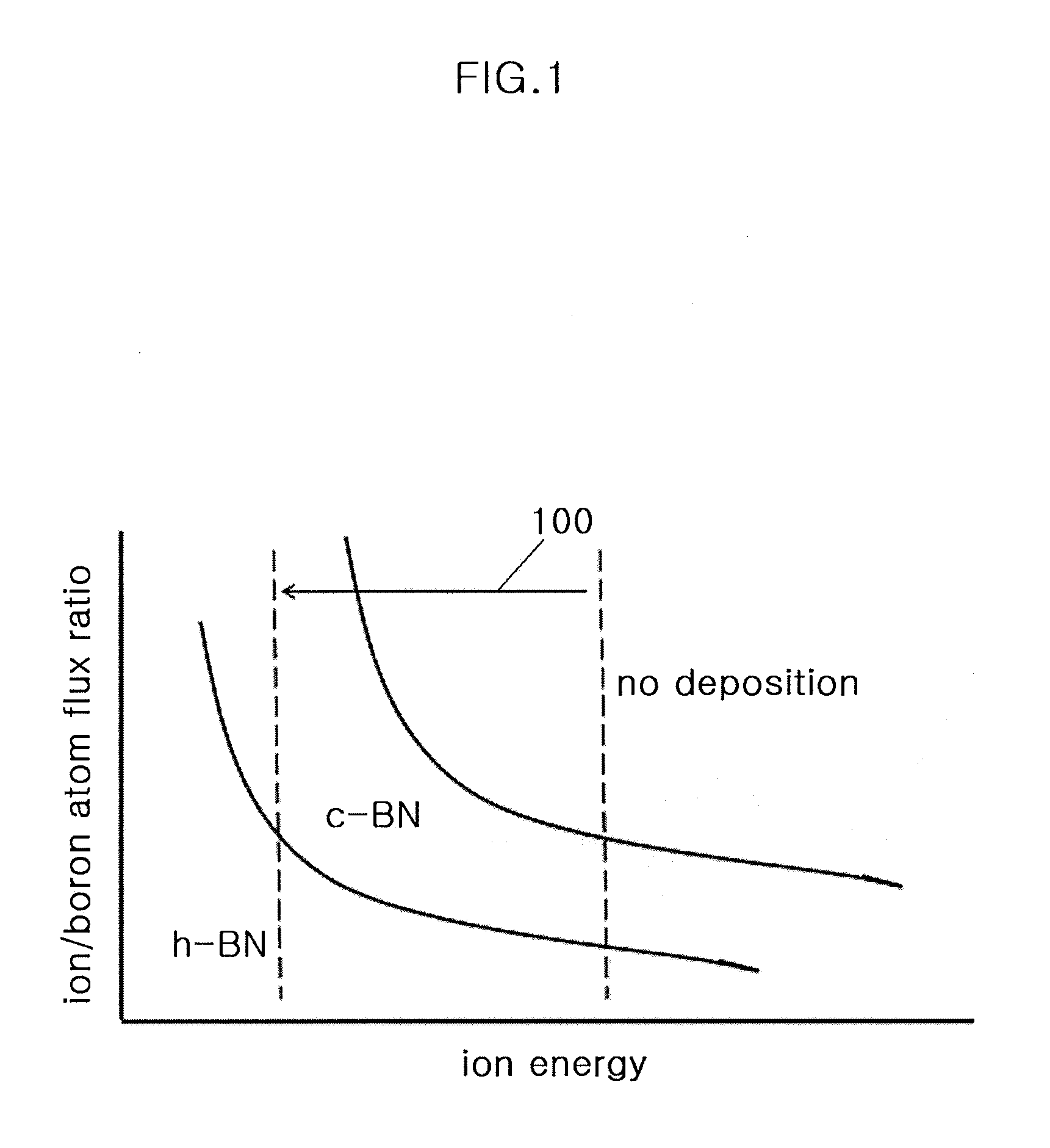
As the ion energy increases, the degree of defects that are caused by the bombarded ions in the thin film increases, and residual stress that is applied to the film also increases due to argon (Ar) ions incorporated into the thin film.
However, in this case, there is a shortcoming in that the decrease in deposition rate is unavoidable.
Due to this relationship between the concentration of argon (Ar) ions and the concentration of sputtered neutral particles, it is difficult in the case of sputtering to control the ratio of the flux of argon (Ar) ions relative to the flux of boron (B) atoms.
Thus, the use of self-bias caused by a high-frequency power source is not preferable in terms of residual stress.

Method used


Image

  • Method for manufacturing cubic boron nitride thin film with reduced compressive residual stress and cubic boron nitride thin film manufactured using the same
  • Method for manufacturing cubic boron nitride thin film with reduced compressive residual stress and cubic boron nitride thin film manufactured using the same
  • Method for manufacturing cubic boron nitride thin film with reduced compressive residual stress and cubic boron nitride thin film manufactured using the same

Examples


Embodiment Construction

[0026]Hereinafter, exemplary embodiments of the present invention will be described in further detail with reference to the accompanying drawings.

[0027]Embodiments are directed to a method for manufacturing a cubic boron nitride (c-BN) thin film by forming a cubic phase in the synthesis of a boron nitride (BN) thin film and to a c-BN thin film manufactured using the method. Embodiments are based on a deposition process in which boron (B) and nitrogen (N) atoms are allowed to be incident on a substrate, on which a thin film is to be formed, while the substrate is bombarded with argon (Ar) ions, thereby forming the thin film. Herein, the argon (Ar) ions are attracted to the substrate by a bias voltage applied to the substrate. In the method for forming the c-BN thin film according to embodiments, the c-BN thin film can be formed by an unbalanced magnetron (UBM) sputtering process or other sputtering processes.

[0028]However, these embodiments are only illustrative, and in other embodim...


PUM

PropertyMeasurementUnit
Timeaaaaaaaaaa
Electric potential / voltageaaaaaaaaaa
Residual stressaaaaaaaaaa

Abstract

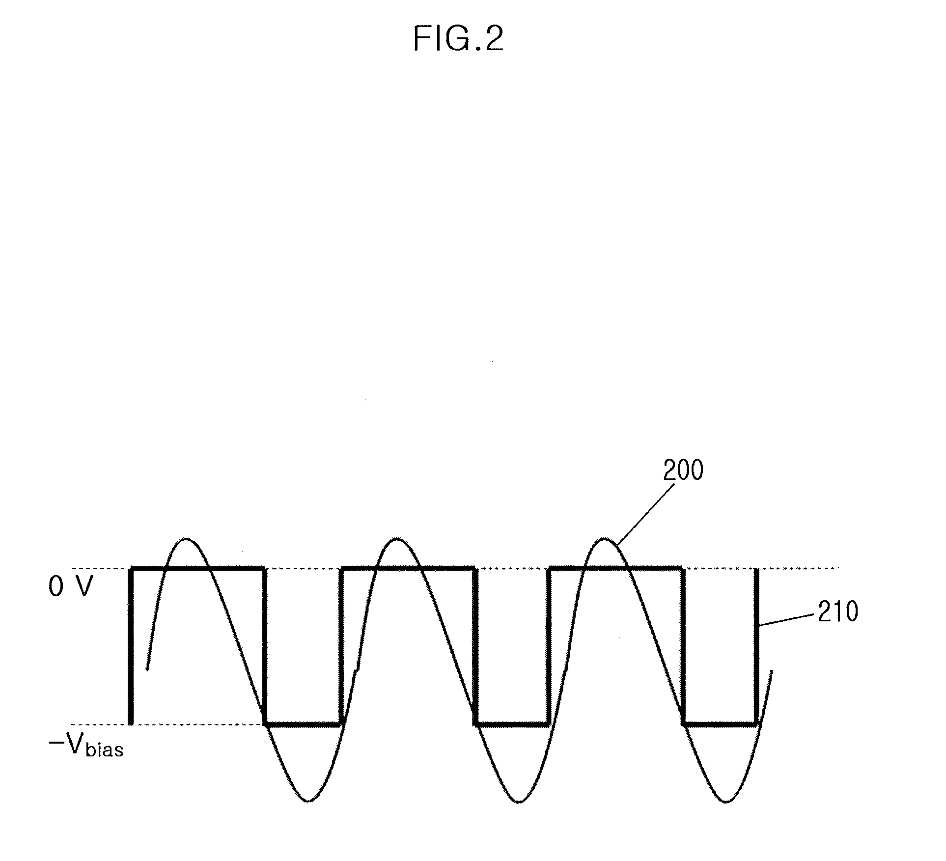
A method for manufacturing a cubic boron nitride (c-BN) thin film includes: applying a pulse-type bias voltage to a substrate; and forming the cubic boron nitride thin film by bombarding the substrate with ions using the pulse-type bias voltage. To control the compressive residual stress of the cubic boron nitride thin film, ON / OFF time ratio of the pulse-type bias voltage may be controlled. The compressive residual stress that is applied to the thin film can be minimized by using the pulse-type voltage as a negative bias voltage applied to the substrate. In addition, the deposition of the c-BN thin film can be performed in a low ion energy region by increasing the ion / neutral particle flux ratio through the control of the ON / OFF time ratio of the pulse-type voltage.

Description

CROSS-REFERENCE TO RELATED APPLICATION[0001]This application claims priority to Korean Patent Application No. 10-2013-0023277, filed on Mar. 5, 2013, and all the benefits accruing therefrom under 35 U.S.C. §119, the contents of which in its entirety are herein incorporated by reference.BACKGROUND[0002]1. Field[0003]Exemplary embodiments relate to a method for manufacturing a cubic boron nitride (c-BN) thin film and a c-BN thin film manufactured using the same, and more particularly to a method for manufacturing a c-BN thin film having a strong adhesion caused by reducing the formation of a compressive residual stress which is applied to the c-BN thin film deposited by sputtering or the like.[0004]2. Description of the Related Art[0005]Cubic boron nitride (c-BN) has properties similar to those of diamond, which has extreme hardness and thermal conductivity. In addition, cubic boron nitride (c-BN) has excellent oxidation resistance, high-temperature stability and reaction stability fo...

Claims


Application Information

Patent Timeline
IPC IPC(8): C23C16/34
CPCC23C16/342C23C14/0647C23C14/345C23C14/06C23C14/34
Inventor BAIK, YOUNG JOONPARK, JONG-KEUKLEE, WOOK SEONG
Owner KOREA INST OF SCI & TECH
Why Eureka
Eureka Blog
Learn More