Semiconductor device and manufacturing method thereof
a semiconductor and manufacturing method technology, applied in semiconductor devices, instruments, electrical devices, etc., can solve the problems of reducing the aperture ratio of the pixel and deteriorating the display quality of the image, and achieve the effect of reducing power consumption, increasing charge capacity, and high aperture ratio
- Summary
- Abstract
- Description
- Claims
- Application Information
AI Technical Summary
Benefits of technology
Problems solved by technology
Method used
Image

Examples
embodiment 1
[0085]In this embodiment, a semiconductor device that is one embodiment of the present invention will be described with reference to drawings. Note that in this embodiment, a liquid crystal display device will be described as an example of the semiconductor device of one embodiment of the present invention. Note that the semiconductor device of one embodiment of the present invention can be used for other display devices.
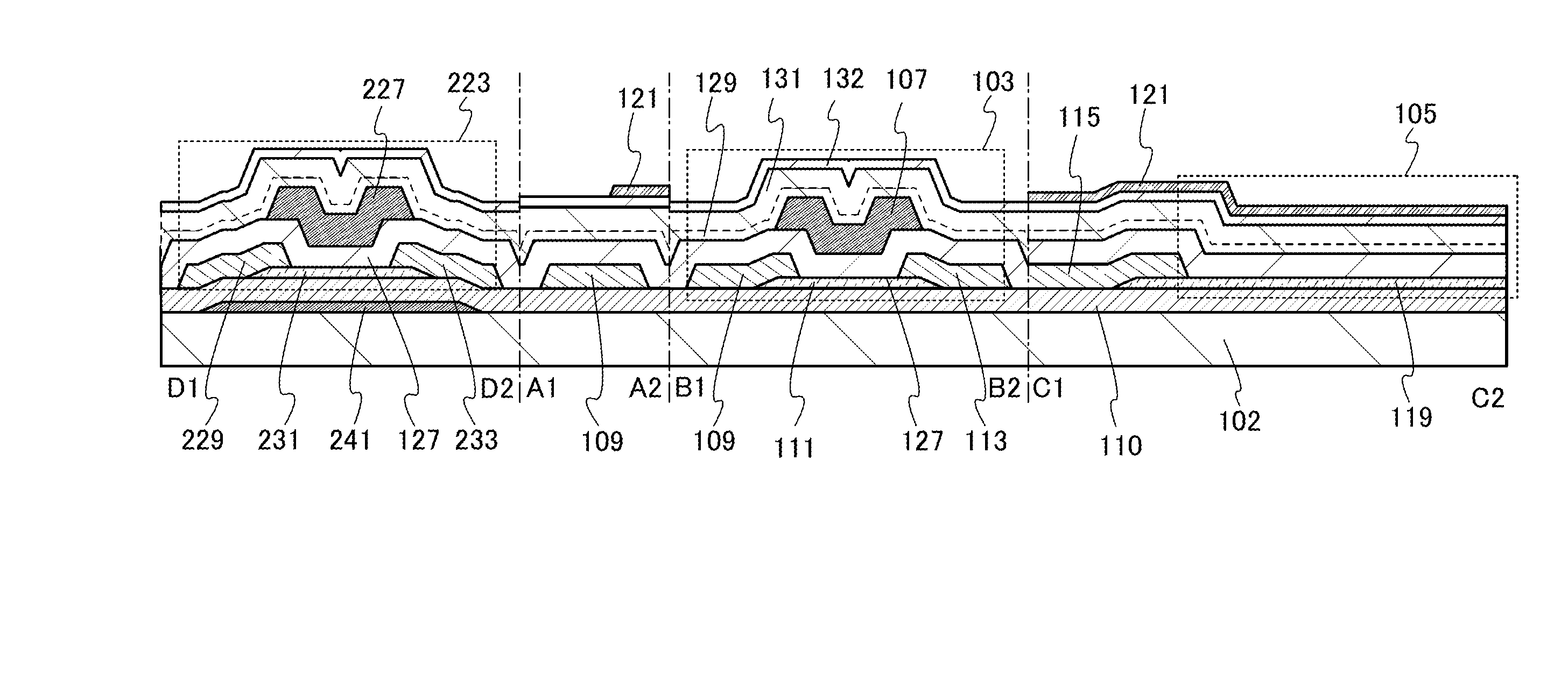
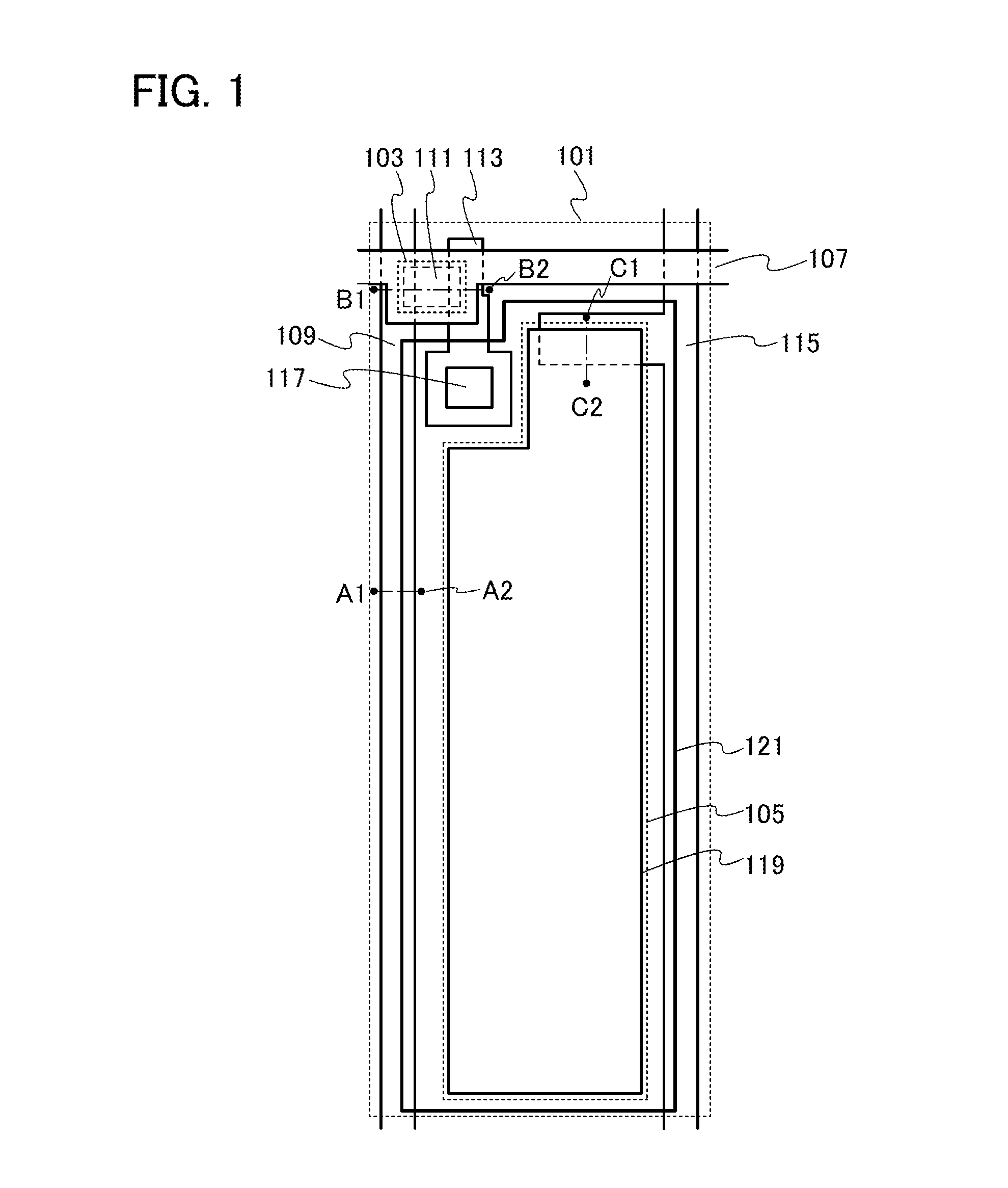
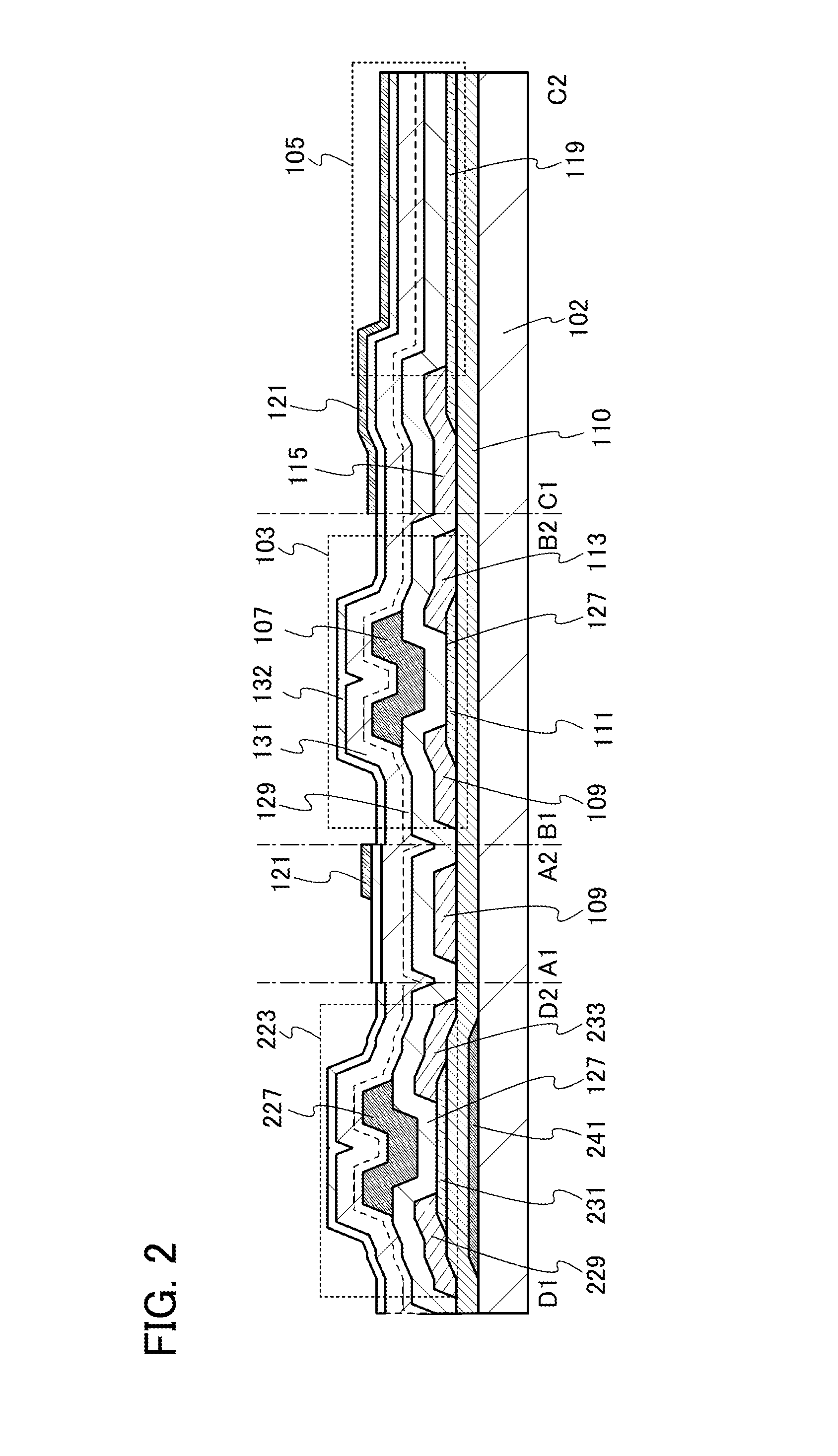
[0086]FIG. 3 illustrates an example of the semiconductor device of one embodiment of the present invention. The semiconductor device illustrated in FIG. 3 includes a pixel portion 100; a first driver circuit 104; a second driver circuit 106; m scan lines 107 which are arranged in parallel or almost in parallel to each other and whose potentials are controlled by the first driver circuit 104; and n signal lines 109 which are arranged in parallel or almost in parallel to each other and whose potentials are controlled by the second driver circuit 106. The pixel portion...
embodiment 2
[0214]Described in this embodiment is one mode of an oxide semiconductor film which can be used as a semiconductor film in the transistor and the capacitor included in the semiconductor device described in the above embodiment.
[0215]An oxide semiconductor may include a non-single-crystal. The non-single-crystal is, for example, structured by at least one of c-axis aligned crystal (CAAC), polycrystal, microcrystal, and an amorphous part.
[0216]An oxide semiconductor may include CAAC. Note that an oxide semiconductor including CAAC is referred to as a CAAC-OS (c-axis aligned crystalline oxide semiconductor).
[0217]In an image obtained with a transmission electron microscope (TEM), crystal parts can be found in the CAAC-OS in some cases. In most cases, in an image obtained with a TEM, crystal parts in the CAAC-OS each fit inside a cube whose one side is less than 100 nm. In an image obtained with a TEM, a boundary between the crystal parts in the CAAC-OS is not clearly observed in some c...
embodiment 3
[0282]Described in this embodiment are the electron diffraction pattern and localized states of a nanocrystalline oxide semiconductor film that can be used in one embodiment of the present invention.
[0283]When a nanocrystalline oxide semiconductor film is observed with electron diffraction (nanobeam electron diffraction) with a beam diameter of 10 nmφ or less, spots without directionality are found in the electron diffraction pattern thereof. This electron diffraction pattern of the nanocrystalline oxide semiconductor film is neither a halo pattern indicating an amorphous state nor a pattern with regular spots indicating a crystal state in which crystals are aligned in a specific surface.
[0284]FIG. 13A shows a cross-sectional transmission electron microscopy (TEM) image of the nanocrystalline oxide semiconductor film. FIGS. 13B, 13C, and 13D show electron diffraction patterns on points 1, 2, and 3 in FIG. 13A, respectively, which are observed by nanobeam electron diffraction.
[0285]I...
PUM
 Abstract
Description
Claims
Application Information
 - R&D
- Intellectual Property
- Life Sciences
- Materials
- Tech Scout
- Unparalleled Data Quality
- Higher Quality Content
- 60% Fewer Hallucinations
Browse by: Latest US Patents, China's latest patents, Technical Efficacy Thesaurus, Application Domain, Technology Topic, Popular Technical Reports.
© 2025 PatSnap. All rights reserved.Legal|Privacy policy|Modern Slavery Act Transparency Statement|Sitemap|About US| Contact US: help@patsnap.com